
Community hub
Recent from talks
Contribute something
Nothing was collected or created yet.
Integrated circuit packaging
View on Wikipedia


Integrated circuit packaging is the final stage of semiconductor device fabrication, in which the die is encapsulated in a supporting case that prevents physical damage and corrosion. The case, known as a "package", supports the electrical contacts which connect the device to a circuit board.
The packaging stage is followed by testing of the integrated circuit.
Design considerations
[edit]
Electrical
[edit]The current-carrying traces that run out of the die, through the package, and into the printed circuit board (PCB) have very different electrical properties compared to on-chip signals. They require special design techniques and need much more electric power than signals confined to the chip itself. Therefore, it is important that the materials used as electrical contacts exhibit characteristics like low resistance, low capacitance and low inductance.[1] Both the structure and materials must prioritize signal transmission properties, while minimizing any parasitic elements that could negatively affect the signal.
Controlling these characteristics is becoming increasingly important as the rest of technology begins to speed up. Packaging delays have the potential to make up almost half of a high-performance computer's delay, and this bottleneck on speed is expected to increase.[1]
Mechanical and thermal
[edit]The integrated circuit package must resist physical breakage, keep out moisture, and also provide effective heat dissipation from the chip. Moreover, for RF applications, the package is commonly required to shield electromagnetic interference, that may either degrade the circuit performance or adversely affect neighboring circuits. Finally, the package must permit interconnecting the chip to a PCB.[1] The materials of the package are either plastic (thermoset or thermoplastic), metal (commonly Kovar) or ceramic. A common plastic used for this is epoxy-cresol-novolak (ECN).[2] All three material types offer usable mechanical strength, moisture and heat resistance. Nevertheless, for higher-end devices, metallic and ceramic packages are commonly preferred due to their higher strength (which also supports higher pin-count designs), heat dissipation, hermetic performance, or other reasons. Generally, ceramic packages are more expensive than similar plastic packages.[3]
Some packages have metallic fins to enhance heat transfer, but these take up space. Larger packages also allow for more interconnecting pins.[1]
Economic
[edit]Cost is a factor in selection of integrated circuit packaging. Typically, an inexpensive plastic package can dissipate heat up to 2W, which is sufficient for many simple applications, though a similar ceramic package can dissipate up to 50W in the same scenario.[1] As the chips inside the package get smaller and faster, they also tend to get hotter. As the subsequent need for more effective heat dissipation increases, the cost of packaging rises along with it. Generally, the smaller and more complex the package needs to be, the more expensive it is to manufacture.[3] Wire bonding can be used instead of techniques such as flip-chip to reduce costs.[4]
History
[edit]
Early integrated circuits were packaged in ceramic flat packs, which the military used for many years for their reliability and small size. The other type of packaging used in the 1970s, called the ICP (Integrated Circuit Package), was a ceramic package (sometimes round as the transistor package), with the leads on one side, co-axially with the package axis.
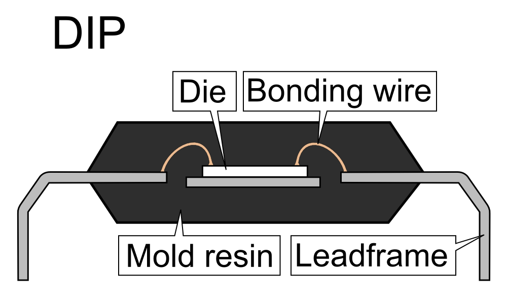
Commercial circuit packaging quickly moved to the dual in-line package (DIP), first in ceramic and later in plastic.[5] In the 1980s VLSI pin counts exceeded the practical limit for DIP packaging, leading to pin grid array (PGA) and leadless chip carrier (LCC) packages.[6] Surface mount packaging appeared in the early 1980s and became popular in the late 1980s, using finer lead pitch with leads formed as either gull-wing or J-lead, as exemplified by small-outline integrated circuit—a carrier which occupies an area about 30–50% less than an equivalent DIP, with a typical thickness that is 70% less.[6]

The next big innovation was the area array package, which places the interconnection terminals throughout the surface area of the package, providing a greater number of connections than previous package types where only the outer perimeter is used. The first area array package was a ceramic pin grid array package.[1] Not long after, the plastic ball grid array (BGA), another type of area array package, became one of the most commonly used packaging techniques.[7]
In the late 1990s, plastic quad flat pack (PQFP) and thin small-outline packages (TSOP) replaced PGA packages as the most common for high pin count devices,[1] though PGA packages are still often used for microprocessors. However, industry leaders Intel and AMD transitioned in the 2000s from PGA packages to land grid array (LGA) packages.[8]
Ball grid array (BGA) packages have existed since the 1970s, but evolved into flip-chip ball grid array (FCBGA) packages in the 1990s. FCBGA packages allow for much higher pin count than any existing package types. In an FCBGA package, the die is mounted upside-down (flipped) and connects to the package balls via a substrate that is similar to a printed-circuit board rather than by wires. FCBGA packages allow an array of input-output signals (called Area-I/O) to be distributed over the entire die rather than being confined to the die periphery.[9] Ceramic substrates for BGA were replaced with organic substrates to reduce costs and use existing PCB manufacturing techniques to produce more packages at a time by using larger PCB panels during manufacturing.[10]
Traces out of the die, through the package, and into the printed circuit board have very different electrical properties, compared to on-chip signals. They require special design techniques and need much more electric power than signals confined to the chip itself.
Recent developments consist of stacking multiple dies in single package called SiP, for System In Package, or three-dimensional integrated circuit. Combining multiple dies on a small substrate, often ceramic, is called an MCM, or Multi-Chip Module. The boundary between a big MCM and a small printed circuit board is sometimes blurry.[11]
Common package types
[edit]

Operations
[edit]For traditional ICs, after wafer dicing, the die is picked from the diced wafer using a vacuum tip or suction cup[12][13] and undergoes die attachment which is the step during which a die is mounted and fixed to the package or support structure (header).[14] In high-powered applications, the die is usually eutectic bonded onto the package, using e.g. gold-tin or gold-silicon solder (for good heat conduction). For low-cost, low-powered applications, the die is often glued directly onto a substrate (such as a printed wiring board) using an epoxy adhesive. Alternatively dies can be attached using solder. These techniques are usually used when the die will be wire bonded; dies with flip chip technology do not use these attachment techniques.[15][16]
IC bonding is also known as die bonding, die attach, and die mount.[17]
The following operations are performed at the packaging stage, as broken down into bonding, encapsulation, and wafer bonding steps. Note that this list is not all-inclusive and not all of these operations are performed for every package, as the process is highly dependent on the package type.
- IC bonding
- IC encapsulation
- Wafer bonding
Sintering die attach is a process that involves placing the semiconductor die onto the substrate and then subjecting it to high temperature and pressure in a controlled environment.[18]
See also
[edit]References
[edit]- ^ a b c d e f g Rabaey, Jan (2007). Digital Integrated Circuits (2nd ed.). Prentice Hall, Inc. ISBN 978-0130909961.
- ^ Ardebili, Haleh; Pecht, Michael G. (2009). "Plastic Encapsulant Materials". Encapsulation Technologies for Electronic Applications. pp. 47–127. doi:10.1016/B978-0-8155-1576-0.50006-1. ISBN 9780815515760. S2CID 138753417 – via ResearchGate.
- ^ a b Greig, William (2007). Integrated Circuit Packaging, Assembly and Interconnections. Springer Science & Business Media. ISBN 9780387339139.
- ^ "Wire Bond Vs. Flip Chip Packaging | Semiconductor Digest". 10 December 2016.
- ^ Dummer, G.W.A. (1978). Electronic Inventions and Discoveries (2nd ed). Pergamon Press. ISBN 0-08-022730-9.
- ^ a b Baker, R. Jacob (2010). CMOS: Circuit Design, Layout, and Simulation, Third Edition. Wiley-IEEE. ISBN 978-0-470-88132-3.
- ^ Ken Gilleo (2003). Area array packaging processes for BGA, Flip Chip, and CSP. McGraw-Hill Professional. p. 251. ISBN 0-07-142829-1.
- ^ "Land Grid Array (LGA) Socket and Package Technology" (PDF). Intel. Retrieved April 7, 2016.
- ^ Riley, George (2009-01-30). "Flipchips: Tutorial #1". Archived from the original on January 30, 2009. Retrieved 2016-04-07.
- ^ Materials for Advanced Packaging. Springer. 17 December 2008. ISBN 978-0-387-78219-5.
- ^ R. Wayne Johnson, Mark Strickland and David Gerke, NASA Electronic Parts and Packaging Program. "3-D Packaging: A Technology Review." June 23, 2005. Retrieved July 31, 2015
- ^ Die Attachment, Fluid Dispensing catalog from SPT small precision tools
- ^ "Die bonding techniques and methods". 9 July 2012.
- ^ L. W. Turner (ed), Electronics Engineers Reference Book, Newnes-Butterworth, 1976, ISBN 0-408-00168-2, pages 11-34 through 11-37
- ^ "Die bonding techniques and methods". 9 July 2012.
- ^ Lau, John H. (30 June 1994). Chip on Board: Technology for Multichip Modules. Springer. ISBN 978-0-442-01441-4.
- ^ "What is the Die Attach process?". Oricus Semicon Solutions. 2021-11-01. Retrieved 2024-04-22.
- ^ Buttay, Cyril, et al. "Die attach of power devices using silver sintering-bonding process optimization and characterization." HiTEN 2011. 2011.