Hubbry Logo
Instruction cycleInstruction cycleMain
Open search
Instruction cycle
Community hub
Instruction cycle
logo
8 pages, 0 posts
0 subscribers
Be the first to start a discussion here.
Instruction cycle
Instruction cycle
from Wikipedia

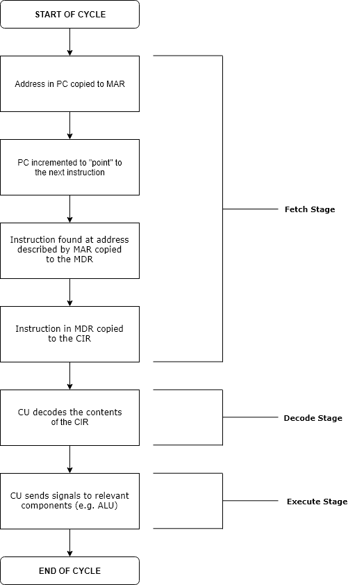
The instruction cycle (also known as the fetch–decode–execute cycle, or simply the fetch–execute cycle) is the cycle that the central processing unit (CPU) follows from boot-up until the computer has shut down in order to process instructions. It is composed of three main stages: the fetch stage, the decode stage, and the execute stage.

This is a simple diagram illustrating the individual stages of the fetch-decode-execute cycle. Legend:

In simpler CPUs, the instruction cycle is executed sequentially, each instruction being processed before the next one is started. In most modern CPUs, the instruction cycles are instead executed concurrently, and often in parallel, through an instruction pipeline: the next instruction starts being processed before the previous instruction has finished, which is possible because the cycle is broken up into separate steps.[1]

Role of components

[edit]

Program counter

[edit]

The program counter (PC) is a register that holds the memory address of the next instruction to be executed. After each instruction copy to the memory address register (MAR), the PC can either increment the pointer to the next sequential instruction, jump to a specified pointer, or branch conditionally to a specified pointer.[2] Also, during a CPU halt, the PC holds the instruction being executed, until an external interrupt or a reset signal is received.

Memory address register

[edit]

The MAR is responsible for storing the address describing the location of the instruction. After a read signal is initiated, the instruction in the address from the MAR is read and placed into the memory data register (MDR), also known as Memory Buffer Register (MBR). This component overall functions as an address buffer for pointing to locations in memory.

Memory data register

[edit]

The MDR is responsible for temporarily holding instructions read from the address in MAR. It acts as a two-way register in the instruction cycle because it can take output from memory to the CPU, or output from the CPU to memory.

Current instruction register

[edit]

The current instruction register (CIR, though sometimes referred to as the instruction register, IR) is where the instruction is temporarily held, for the CPU to decode it and produce correct control signals for the execution stage.

Control unit

[edit]

The control unit (CU) decodes the instruction in the current instruction register (CIR). Then, the CU sends signals to other components within the CPU, such as the arithmetic logic unit (ALU), or back to memory to fetch operands, or to the floating-point unit (FPU). The ALU performs arithmetic operations based on specific opcodes in the instruction. For example, in RISC-V architecture, funct3 and funct7 opcodes exist to distinguish whether an instruction is a logical or arithmetic operation.

Summary of stages

[edit]

Each computer's CPU can have different cycles based on different instruction sets, but will be similar to the following cycle:[3]

  1. Fetch stage: The fetch stage initiates the instruction cycle by retrieving the next instruction from memory. During this stage, the PC is polled for the address of the instruction in memory (using the MAR). Then the instruction is stored from the MDR into the CIR. At the end of this stage, the PC points to the next instruction that will be read at the next cycle.
  2. Decode stage: During this stage, the encoded instruction in the CIR is interpreted by the CU. It determines what operations and additional operands are required for execution and sends respective signals to respective components within the CPU, such as the ALU or FPU, to prepare for the execution of the instruction.
  3. Execute stage: This is the stage where the actual operation specified by the instruction is carried out by the relevant functional units of the CPU. Logical or arithmetic operations may be run by the ALU, data may be read from or written to memory, and the results are stored in registers or memory as required by the instruction. Based on output from the ALU, the PC might branch.
  4. Repeat cycle

In addition, on most processors, interrupts can occur. This will cause the CPU to jump to an interrupt service routine, execute that, and then return to the instruction it was meant to be executing. In some cases, the instruction can be interrupted in the middle, but there will be no effect, and the instruction will be re-executed after return from the interrupt.

Initiation

[edit]

The first instruction cycle begins as soon as power is applied to the system, with an initial PC value that is predefined by the system's architecture (for instance, in Intel IA-32 CPUs, the predefined PC value is 0xfffffff0 whereas for ARM architecture CPUs, it is 0x00000000.) Typically, this address points to a set of instructions in read-only memory (ROM), which begins the process of loading (or booting) the operating system.[4]

Fetch stage

[edit]

The fetch stage is the same for each instruction:

  1. The PC contains the address of the instruction to be fetched.
  2. This address is copied to the MAR, where this address is used to poll for the location of the instruction in memory.
  3. The CU sends a signal to the control bus to read the memory at the address in MAR - the data read is placed in the data bus.[5]
  4. The data is transferred to the CPU via the data bus, where it's loaded into the MDR - at this stage, the PC increments by one.
  5. The contents (instruction to-be-executed) of the MDR are copied into the CIR (where the instruction opcode and data operand can be decoded).

Decode stage

[edit]

The decoding process allows the processor to determine what instruction is to be performed so that the CPU can tell how many operands it needs to fetch in order to perform the instruction. The opcode fetched from the memory is decoded for the next steps and moved to the appropriate registers. The decoding is typically performed by binary decoders in the CPU's CU.[6]

Determining effective addresses

[edit]

There are various ways that an architecture can specify determining the address for operands, usually called the addressing modes.[7]

Some common ways the effective address can be found are:

  • Direct addressing - the address of the instruction contains the effective address
  • Indirect addressing - the address of the instruction specifies the address of the memory location that contains the effective address
  • PC-relative addressing - the effective address is calculated from an address relative to the PC
  • Stack addressing - the operand is at the top of the stack

Execute stage

[edit]

The CPU sends the decoded instruction (decoded from the CU) as a set of control signals to corresponding components. Depending on the type of instruction, any of these can happen:

  • Arithmetic/logical operations can be executed by the ALU (for example, ADD, SUB, AND, OR)[8]
  • Read/writes from memory can be executed (for example, loading/storing bytes)
  • Control flow alterations can be executed (for example, jumps or branches) - at this stage, if a jump were to occur, instead of the PC incrementing to the adjacent pointer, it would jump to the pointer specified in the instruction

This is the only stage of the instruction cycle that is useful from the perspective of the end-user. Everything else is overhead required to make the execute step happen.

See also

[edit]

References

[edit]
Revisions and contributorsEdit on WikipediaRead on Wikipedia
from Grokipedia
The instruction cycle, also known as the fetch-decode-execute cycle, is the fundamental process by which a computer's (CPU) retrieves, interprets, and carries out instructions from a program stored in main , repeating continuously to execute software. This cycle forms the core of CPU operation in von Neumann architectures, where instructions and data share the same memory space, enabling sequential program execution. The cycle typically consists of three primary phases: fetch, where the CPU uses the (PC) to load the next instruction from memory into the (IR) and increments the PC for the subsequent instruction; decode, in which the analyzes the instruction's and operands to generate the necessary control signals for execution; and execute, during which the CPU performs the specified operation, such as arithmetic computations via the (ALU), data transfers to or from memory, or changes like branching. Each phase is synchronized by the CPU's clock, ensuring orderly progression, though the exact timing and sub-steps vary by architecture—for instance, indirect addressing may add an extra memory access during execution. In practice, the instruction cycle may include additional elements, such as an interrupt cycle to handle external events like I/O requests by temporarily suspending the current program, storing the return address, and branching to an . Modern CPUs optimize this basic cycle through techniques like pipelining, which overlaps phases across multiple instructions to increase throughput, and caching to reduce memory access latency, though these do not alter the underlying fetch-decode-execute model. The cycle's efficiency directly impacts overall system performance, as each instruction requires one or more full cycles, influencing metrics like (CPI).

Introduction

Definition and overview

The instruction cycle, also known as the fetch-decode-execute cycle, is the fundamental operational process of a (CPU) in which it repeatedly retrieves an instruction from main memory, interprets its meaning, and performs the specified action, continuing this loop until the program ends or an occurs. This cycle forms the core mechanism for executing programs, enabling the CPU to process sequences of instructions stored in memory. At a high level, the cycle comprises three interdependent stages: in the fetch stage, the CPU uses the program counter to locate and load the next instruction into the instruction register; the decode stage analyzes the instruction to identify the operation and required operands; and the execute stage carries out the operation, such as arithmetic computation or data movement, while updating the program counter for the next iteration. These stages are tightly coupled, as the output of one directly informs the next— for instance, decoding determines the execution path—ensuring orderly program flow and efficient resource use within the CPU. The instruction cycle is a key element of the , which stores both program instructions and data in a shared, unified space, allowing the CPU to fetch and process them interchangeably via addresses. This design, originating from early stored-program concepts, facilitates flexible program execution but introduces potential bottlenecks due to the single bus handling both instruction fetches and data accesses.

Importance and historical context

The instruction cycle's historical roots trace back to the early electronic computers of the 1940s, where machines like the required extensive manual intervention for programming. Completed in 1945, the relied on physical rewiring of patch cables and manual setting of switches to configure operations, a process that could take days for each new program and limited its flexibility for automated computation. This labor-intensive approach highlighted the need for a more efficient paradigm, paving the way for the stored-program concept outlined in John von Neumann's 1945 report on the . In this seminal document, von Neumann proposed a design where both instructions and data reside in the same memory, enabling the CPU to sequentially fetch, decode, and execute instructions without manual reconfiguration, thus establishing the foundational fetch-decode-execute model. The significance of the instruction cycle lies in its role in enabling fully automated program execution, transforming computers from specialized calculators into general-purpose machines capable of running complex software dynamically. By storing programs in memory alongside data, the cycle allows the CPU to process instructions in a repeatable loop, drastically reducing setup time and human error compared to earlier wired-program systems. This automation not only streamlined computational workflows but also optimized resource efficiency within the CPU, as the control logic coordinates memory access, decoding, and execution in a synchronized manner, minimizing idle time and maximizing throughput for given hardware constraints. The model's emphasis on sequential instruction handling became the bedrock for resource management in processors, ensuring that computational power is allocated effectively across diverse workloads. A key milestone in the instruction cycle's evolution occurred in the 1950s with the introduction of dedicated control units in commercial computers, exemplified by IBM's 701 in 1952. The 701's Electronic Analytic Control Unit automated the orchestration of the fetch-decode-execute sequence through stored-program instructions, marking the first mass-produced implementation of this fully automated cycle and bridging theoretical designs to practical engineering. This advancement solidified the instruction cycle as the universal foundation for all modern processors, underpinning everything from resource-constrained microcontrollers in embedded systems to high-performance supercomputers handling petascale simulations, and remains integral to contemporary CPU architectures despite subsequent optimizations.

Hardware Components

Program counter

The program counter (PC), also known as the in some architectures, is a dedicated register within the (CPU) that stores the of the next instruction to be fetched from main memory during program execution. This register ensures sequential processing of instructions by maintaining a precise pointer to the program's current position in memory. In typical operation, after an instruction is fetched, the program counter is incremented by the length of that instruction to advance to the subsequent one, facilitating linear program flow. For example, in byte-addressable systems with fixed-length 32-bit instructions, such as those in the , the PC increments by 4 bytes. During the fetch process, the PC's value is briefly transferred to the to initiate retrieval of the instruction from the specified . The also plays a critical role in non-sequential execution through instructions, where it is loaded with a new address rather than incremented, enabling branches, jumps, or subroutine calls. For instance, an unconditional jump instruction directly overwrites the PC with the target address, altering the program's execution path to a different location. This mechanism supports conditional logic, loops, and function invocations essential to .

Memory address register

The memory address register (MAR) is a special-purpose register within the (CPU) that temporarily holds the to be accessed during read or write operations, latching this address from sources such as the or the (ALU) output to facilitate communication with main memory. This latching ensures that the address remains stable while the memory system processes the request, preventing timing errors in the data path. In the instruction cycle, the MAR plays a critical role during the fetch by being loaded with the current value from the , which specifies the location of the next instruction in , enabling the CPU to retrieve it accurately. During the execute , the MAR is similarly utilized when operand addresses—often computed by the ALU based on the instruction—are transferred to it, allowing the CPU to access necessary data from main for operations like loading or storing values. This dual usage underscores the MAR's function as a bridge between internal CPU computations and external memory interactions. The operation of the MAR is tightly synchronized with the system clock, where address values are latched on rising or falling clock edges to provide stable signals to modules, adhering to the required setup and hold times for reliable access. This clock-driven timing prevents address glitches and ensures that operations complete within the allotted cycle periods, contributing to the overall efficiency of the instruction execution process.

Memory data register

The memory data register (MDR), also known as the , is a special-purpose bidirectional register within the (CPU) that temporarily holds data or instructions being transferred to or from the main . It serves as an intermediary buffer to facilitate efficient memory operations, ensuring that the CPU can access or store information without directly interfacing with the slower main during each transaction. This design allows the MDR to function in both input and output roles: receiving data from during read operations or providing data to during write operations. In the fetch stage of the instruction cycle, the MDR plays a critical role by capturing the instruction retrieved from memory once the memory address register (MAR) has signaled the appropriate location. The memory system then transfers the instruction word into the MDR, from where it is subsequently forwarded to the current instruction register (CIR) for decoding. This buffering prevents the need for immediate processing while the memory access completes, maintaining the cycle's efficiency. The MDR works in tandem with the MAR to complete these read transactions, where the MAR provides the address and the MDR handles the content. During the execute stage, the MDR is essential for memory-bound operations such as load and store instructions, where it temporarily stores operands fetched from or holds results to be written back. For a load operation, read from enters the MDR before being routed to the appropriate general-purpose register; conversely, for stores, the data from a CPU register is placed into the MDR prior to writing it to the specified address. This dual functionality ensures seamless movement without stalling the CPU's processing .

Current instruction register

The current instruction register, also known as the (IR), serves as a dedicated storage element in the CPU's that holds the raw machine instruction recently fetched from , encompassing the and operands in their unprocessed binary form. This register ensures the instruction is readily available for subsequent processing without repeated access. During the fetch stage, the IR receives the instruction directly from the memory register (MDR) once the memory read operation concludes, and it retains this content stably through the decode phase to support controlled execution flow. This transfer isolates the instruction from general pathways, optimizing CPU efficiency. The IR's design accounts for instruction format variations across architectures: in CISC systems like x86, it manages variable-length instructions that can range from 1 to 15 bytes, requiring flexible buffering during fetch, while RISC architectures employ fixed-length formats, such as 32 or 64 bits, simplifying IR sizing and access.

Control unit

The (CU) is the component of the (CPU) responsible for directing the flow of data between the processor's (ALU), registers, and memory by generating a sequence of control signals that orchestrate the timing and paths of operations during the instruction cycle. These signals ensure that each stage of the instruction cycle—such as fetching an instruction, decoding its , and executing the required actions—proceeds in the correct order without overlap or conflict. The CU interprets the from the current and issues precise commands to enable or disable hardware elements, maintaining through a . Control signals produced by the CU include memory read/write enables, which control data transfer to and from main ; ALU operation selects, specifying functions like addition or logical AND; and register load/strobe signals, which determine when data is latched into specific registers. These signals are derived combinatorially or sequentially based on the decoded , ensuring that only the necessary hardware paths are activated for the current instruction. For instance, during the fetch stage, the CU might assert a memory read signal to load the instruction into the register, while in execution, it could enable ALU inputs from registers and output to a destination. The reliance on the current provides the input that drives this signal generation process during decoding. There are two primary implementations of the : hardwired and microprogrammed. A hardwired is constructed using circuits and flip-flops to form a state machine, where control signals are generated directly from the current state and via fixed equations; this approach offers high speed due to minimal propagation delays, making it suitable for simple CPUs with reduced instruction set computing (RISC) architectures. In contrast, a microprogrammed stores sequences of microinstructions in a (ROM) or control store, where each microinstruction specifies a set of control signals for one clock cycle; this method provides greater flexibility for modifying instruction behaviors through updates, which is advantageous in complex CPUs with complex instruction set computing (CISC) designs, such as early mainframes. Hardwired units excel in performance-critical simple processors, while microprogrammed units dominated in systems requiring adaptability, like the series.

Stages of the Instruction Cycle

Initiation

The initiation phase of the instruction cycle begins with the CPU's response to a or system reset signal, which initializes the processor to a known state and prepares it for executing the first instruction. During this process, the hardware automatically sets the (PC) to a fixed that points to the of , such as in x86 systems or a reset handler in architectures. For instance, in x86 processors, the reset sets the instruction pointer (EIP) to 0000FFF0h and the code segment (CS) selector to F000h, resulting in a physical starting address of FFFFFFF0h in real-address mode, where the entry code resides. Similarly, in processors, the base is typically set to 0x00000000, with the initial stack pointer loaded from this location and the PC directed to the reset handler at 0x00000004 for Cortex-M cores, initiating execution. Upon assertion of the reset signal, the activates the initial memory read operation using the preset PC value, thereby triggering the first instruction fetch without any preceding instructions or pipeline state. This hardware-driven activation ensures that the processor begins operation immediately after stabilization of power and clock signals, bypassing any software intervention at this stage. The reset signal propagates through the control logic to enable the bus with the initial PC and assert the memory read control, loading the instruction into the current to commence the cycle. This initiation assumes that system memory already contains valid code at the designated address, with no prior initialization of elements like the stack pointer (beyond its reset value) or general-purpose registers, which remain in their default cleared or undefined states until configures them. Following this setup, the seamlessly transitions to the fetch stage to retrieve and process the initial instruction.

Fetch stage

The fetch stage initiates the retrieval of the next instruction from main memory by utilizing the address held in the (PC). The process starts with the contents of the PC being loaded into the (MAR), which specifies the memory location to access. A read enable signal is then issued to the memory unit, prompting it to fetch the instruction from the addressed location and load it into the memory data register (MDR). Once the memory operation completes, the instruction data from the MDR is transferred to the (CIR), preparing it for subsequent decoding. Finally, the PC is incremented—typically by the length of one instruction, such as 4 bytes in 32-bit systems—to point to the next instruction's address. In terms of timing, the fetch stage in simple single-cycle processors completes within one clock cycle, allowing the entire instruction execution to align with the processor's , such as 1 GHz equating to roughly 1 per stage. However, multi-cycle designs extend this stage across multiple clock cycles to accommodate access latencies and bus transfer delays, ensuring synchronization without stalling the overall . Error handling during the fetch stage often includes basic parity checks on the retrieved instruction to detect bit errors from memory reads or transmission. If a parity mismatch occurs, the processor may trigger an exception or retry mechanism, though implementation varies by . The PC and MAR facilitate this address transfer efficiently, minimizing overhead in the retrieval process.

Decode stage

In the decode stage of the instruction cycle, the examines the stored in the (CIR) to interpret the fetched instruction and determine the required operation. The , typically the initial bits of the instruction word, identifies the specific action, such as an arithmetic operation like ADD or a data transfer like LOAD. For instance, in RISC architectures, the 7-bit field (bits 6:0) distinguishes instruction types, with additional fields like funct3 (bits 14:12) and funct7 (bits 31:25) providing further specificity for operations within the type. This decoding process involves mapping the through a —often implemented as a (PLA) or (ROM)—to recognize the instruction format and initiate operand handling. Once the is identified, the extracts operands from the instruction, which may include immediate values embedded directly in the instruction word or references to registers and locations via addressing modes. Addressing modes dictate how operands are located, with common variants including direct (where the operand is explicitly provided), indirect (where the instruction points to a location containing the actual ), and indexed (combining a base with an offset or index). In the indexed mode, the effective address is calculated as \text{effective_address} = \text{base_register} + \text{offset}, where the base_register holds a value from a general-purpose register and the offset is a sign-extended immediate from the instruction. For example, in load instructions using base/displacement addressing, the 5-bit register specifier (rs1) selects the base register, while a 12-bit immediate field provides the offset, which is sign-extended to 64 bits before addition. This preparation ensures operands are resolved without performing the actual data access, which occurs later. The decode stage concludes by generating control signals that configure the processor for the subsequent execute stage, including selections for the (ALU) operation, memory access type, and register write-back. These signals, such as ALUOp (specifying functions like add or subtract) and ALUSrc (choosing between register or immediate inputs), are derived directly from the decoded opcode and addressing details. For branch instructions, preliminary computations like sign-extending the offset prepare the branch target address as PC + offset, though final evaluation may defer to execution. This signal preparation enables efficient handoff, ensuring the is primed for operation-specific actions without redundant analysis.

Execute stage

In the execute stage of the instruction cycle, the processor carries out the operation specified by the decoded instruction, utilizing control signals generated during the decode phase to direct data flow and computations. The (ALU) performs the core arithmetic or logical operations on the operands retrieved from registers or memory, such as addition where the result is computed as operand1 + operand2 for an ADD instruction. The orchestrates this by routing the operands to the ALU inputs and directing the output to the appropriate destination, which may be a or main memory, ensuring precise execution of the instruction's intent. For branching instructions, the execute stage evaluates conditional logic using ALU results to determine program flow; for instance, a branch-if-equal (BEQ) instruction, as in , subtracts the two source registers and branches to a new address if the result is zero, thereby altering the sequence of subsequent instructions. This mechanism may rely on status flags in some architectures or direct computations in others, such as checking for a zero ALU result to indicate equality. Upon completion of the operation, the execute stage updates the processor status word (PSW) with relevant flags, including , carry, overflow, or bits, which reflect the outcome of the ALU and influence future conditional decisions. The results are prepared for storage or further use, after which the cycle typically loops back to the fetch stage for the next instruction unless the processor encounters a halt condition. This stage ensures the faithful implementation of the instruction's semantics, forming the computational heart of the CPU's operation.

Variations and Extensions

Interrupt handling

Interrupt handling in the instruction cycle refers to the process by which the CPU temporarily suspends the normal fetch-decode-execute sequence to address urgent external or internal events, ensuring responsive system operation without permanent disruption to the primary program. These events, known as interrupts, can originate from hardware sources such as I/O device completion signals (e.g., a disk controller finishing a data transfer) or software sources like arithmetic exceptions (e.g., division by zero). Upon detection, the CPU automatically saves the current program counter (PC) and processor status word (PSW) onto the stack to preserve the interrupted program's state, then transfers control to a dedicated interrupt service routine (ISR) for processing. The ISR, a specialized code segment, executes the necessary actions—such as reading device status, updating system variables, or notifying the operating system—while often saving and restoring additional registers to avoid corrupting the original context. To support vectored interrupts, which enable direct addressing of specific handlers, architectures like x86 employ an interrupt descriptor table (IDT) or IRQ table where each interrupt type maps to a unique vector; for instance, the interrupt controller (e.g., 8259A) provides a vector number that indexes the table to locate the ISR address. In contrast, MIPS uses a fixed entry point at address 0x00000080 for external interrupts, with polling to identify the source. Masking mechanisms, implemented via bits in the status register or PSW, allow higher-priority interrupts to preempt lower ones while disabling non-essential ones during critical sections, such as within an ongoing ISR, to prevent nesting overload. Upon completion of the ISR, a special return-from-interrupt instruction (e.g., IRET in x86 or ERET in MIPS) restores the saved PC and PSW from the stack or dedicated registers like the exception PC (EPC), allowing the instruction cycle to resume precisely from the point of interruption. This ensures transparent handling from the program's perspective, maintaining the illusion of uninterrupted execution. Priority levels are typically assigned to interrupt sources—such as level 4 for disk I/O versus level 2 for printers—to resolve conflicts when multiple signals arrive simultaneously, with the CPU or a dedicated arbiter selecting the highest-priority one for immediate service.

Pipelining

Pipelining is a technique in that overlaps the execution of multiple instructions by dividing the instruction cycle into several sequential stages, allowing different instructions to be processed concurrently in an assembly-line fashion. This approach transforms the processor's to handle finer-grained operations, such as the five-stage commonly used in MIPS architectures: Instruction Fetch (IF), Instruction Decode (ID), Execute (EX), Memory Access (MEM), and Write Back (WB). In this setup, while one instruction completes its write-back stage, another is executing arithmetic operations, a third is decoding, and so on, enabling multiple instructions to progress through the simultaneously. The primary benefit of pipelining is a significant increase in CPU throughput, measured as (IPC). In a non-pipelined processor, IPC is typically 1, but an ideal k-stage can achieve an IPC approaching 1 while reducing the clock cycle time, leading to a theoretical of up to k times for long instruction sequences; for instance, a 5-stage can theoretically deliver up to 5 times the of a single-cycle design by completing one instruction per cycle after the pipeline fills. This enhancement stems from the parallelism inherent in processing independent instructions across stages, building on the basic fetch, decode, and execute phases to maximize utilization without increasing the overall latency for individual instructions. Despite these advantages, pipelining introduces challenges known as hazards, which can disrupt the flow and reduce effective throughput. Structural hazards occur when hardware resources, such as memory units, are needed simultaneously by multiple stages, leading to conflicts. Data hazards arise from dependencies between instructions, particularly read-after-write (RAW) cases where a later instruction requires a result not yet available from an earlier one still in the pipeline. Control hazards stem from conditional branches, where the next instruction to fetch depends on an unresolved outcome, potentially causing incorrect instructions to enter the pipeline. To mitigate these hazards, modern pipelines employ techniques like forwarding (also called bypassing), which routes data directly from a producing stage to a consuming one via additional multiplexers, avoiding waits for register writes. Stalling inserts no-operation (NOP) bubbles into the to delay dependent instructions until hazards resolve, ensuring correctness at the cost of cycles. For control hazards, branch prediction speculatively fetches instructions based on likely outcomes (e.g., assuming branches are not taken), flushing the only on mispredictions to minimize penalties. These resolutions balance performance and complexity, with forwarding and prediction often used together to approach ideal IPC in practice.

Architectural differences

The instruction cycle exhibits significant variations between Reduced Instruction Set Computing (RISC) and Complex Instruction Set Computing (CISC) architectures, primarily due to differences in instruction set design that influence fetch, decode, and execute stages. RISC architectures, such as and MIPS, employ fixed-length instructions, typically 32 bits, which simplifies the fetch and decode processes by allowing uniform alignment and rapid parsing without variable boundary detection. This design enables simple decode and execute stages, often completing in a single clock cycle per instruction, and restricts memory operations to dedicated load/store instructions that operate exclusively between registers and memory, avoiding direct memory-to-memory computations. In contrast, CISC architectures like x86 utilize variable-length instructions, ranging from 1 to 15 bytes or more, which complicates the fetch stage as the processor must determine instruction boundaries dynamically and increases decode complexity due to diverse formats and addressing modes. Complex instructions in CISC often span multiple cycles for execution, incorporating memory operations directly within arithmetic or logical commands, and rely on during decoding to translate these into simpler, RISC-like primitive operations for hardware implementation. These architectural choices yield distinct performance implications: RISC's uniformity and simplicity facilitate efficient pipelining by minimizing dependencies and stalls in the instruction cycle, promoting higher throughput in modern processors. Conversely, CISC's emphasis on dense, multifaceted instructions supports with legacy software but demands more sophisticated decode hardware, such as advanced prefetch units and engines, to manage cycle overhead and maintain competitiveness.

References

Add your contribution
Related Hubs
User Avatar
No comments yet.