
Community hub
Recent from talks
Contribute something
Nothing was collected or created yet.
Insulated-gate bipolar transistor
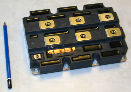
View on Wikipedia IGBT module (IGBTs and freewheeling diodes) with a rated current of 1200 A and a maximum voltage of 3300 V | |
| Working principle | Semiconductor |
|---|---|
| Inventor | 1959 |
| Electronic symbol | |
 IGBT schematic symbol | |
An insulated-gate bipolar transistor (IGBT) is a three-terminal power semiconductor device primarily forming an electronic switch. It was developed to combine high efficiency with fast switching. It consists of four alternating layers (NPNP)[1][2][3][4] that are controlled by a metal–oxide–semiconductor (MOS) gate structure.
Although the structure of the IGBT is topologically similar to a thyristor with a "MOS" gate (MOS-gate thyristor), the thyristor action is completely suppressed, and only the transistor action is permitted in the entire device operation range. It is used in switching power supplies in high-power applications: variable-frequency drives (VFDs) for motor control in trains, electric cars, variable-speed refrigerators and air conditioners, as well as lamp ballasts, arc-welding machines, photovoltaic and hybrid inverters, uninterruptible power supply systems (UPS), and induction stoves.
Since it is designed to turn on and off rapidly, the IGBT can synthesize complex waveforms with pulse-width modulation and low-pass filters, thus it is also used in switching amplifiers in sound systems and industrial control systems. In switching applications, modern devices feature pulse repetition rates well into the ultrasonic-range frequencies, which are at least ten times higher than audio frequencies handled by the device when used as an analog audio amplifier. As of 2010[update], the IGBT was the second most widely used power transistor, after the power MOSFET.[citation needed]
| Device characteristic | Power BJT | Power MOSFET | IGBT |
|---|---|---|---|
| Voltage rating | High <1 kV | High <1 kV | Very high >1 kV |
| Current rating | High <500 A | Low <200 A | High >500 A |
| Input drive | Current ratio hFE ~ 20–200 |
Voltage VGS ~ 3–10 V |
Voltage VGE ~ 4–8 V |
| Input impedance | Low | High | High |
| Output impedance | Low | Medium | Low |
| Switching speed | Slow (μs) | Fast (ns) | Medium |
| Cost | Low | Medium | High |
Device structure
[edit]
An IGBT cell is constructed similarly to an n-channel vertical-construction power MOSFET, except the n+ drain is replaced with a p+ collector layer, thus forming a vertical PNP bipolar junction transistor. This additional p+ region creates a cascade connection of a PNP bipolar junction transistor with the surface n-channel MOSFET. The whole structure comprises a four-layered NPNP.[1][2][3][4]
History
[edit]The bipolar point-contact transistor was invented in December 1947[6] at the Bell Telephone Laboratories by John Bardeen and Walter Brattain under the direction of William Shockley. The junction version known as the bipolar junction transistor (BJT), invented by Shockley in 1948.[7] Later a similar thyristor was proposed by William Shockley in 1950 and developed in 1956 by power engineers at General Electric (GE). The metal–oxide–semiconductor field-effect transistor (MOSFET) was later invented at Bell Labs between 1959 and 1960.[8][9]
The basic IGBT mode of operation, where a pnp transistor is driven by a MOSFET, was first proposed by K. Yamagami and Y. Akagiri of Mitsubishi Electric in the Japanese patent S47-21739, which was filed in 1968.[10]

In 1978 J. D. Plummer and B. Scharf patented a NPNP transistor device combining MOS and bipolar capabilities for power control and switching.[11][12] The development of the IGBT was characterised by an effort to completely suppress the thyristor operation, or the latch-up, in the four-layer device because the latch-up caused fatal device self-destruction. IGBTs had thus been established when the complete suppression of the latch-up of the parasitic thyristor was achieved. Later, Hans W. Becke and Carl F. Wheatley developed a similar device claiming non-latch-up. They patented the device in 1980, referring to it as "power MOSFET with an anode region" for which "no thyristor action occurs under any device operating conditions".[13][14]
A. Nakagawa et al. invented the device design concept of non-latch-up IGBTs in 1984.[15][16] The invention is characterised by the device design setting the device saturation current below the latch-up current, which triggers the parasitic thyristor. This invention achieved complete suppression of the parasitic thyristor action for the first time, because the maximal collector current was limited by the saturation current and never exceeded the latch-up current.
In the early development stage of the IGBT, research was aimed at increasing the latch-up current itself to suppress the latch-up of the parasitic thyristor. However, all these efforts failed because the IGBT could conduct an enormously large current. Successful suppression of latch-up became possible by constraining the maximal collector current to stay below the latch-up current, by controlling or reducing the saturation current of the inherent MOSFET. This was the breakthrough behind the non-latch-up IGBT, which in turn made "Becke’s device" possible.
The IGBT is characterised by its ability to simultaneously handle a high voltage and a large current. The product of the voltage and the current density that the IGBT can handle reached more than 5×10⁵ W/cm2,[17][18] which far exceeded the value, 2×10⁵ W/cm2, of existing power devices such as bipolar transistors and power MOSFETs. This is a consequence of the large safe operating area of the IGBT. The IGBT is the most rugged and the strongest power device yet developed, affording ease of use and so displacing bipolar transistors and even gate turn-off thyristors (GTOs). This excellent feature of the IGBT had suddenly emerged when the non-latch-up IGBT was established in 1984 by solving the problem of so-called "latch-up", which is the main cause of device destruction or device failure. Before that, the developed devices were very weak and were easily destroyed by "latch-up".
Practical devices
[edit]Practical devices capable of operating over an extended current range were first reported by B. Jayant Baliga et al. in 1982.[19] The first experimental demonstration of a practical discrete vertical IGBT device was reported by Baliga at the IEEE International Electron Devices Meeting (IEDM) that year.[20][19] General Electric commercialized Baliga's IGBT device the same year.[21] Baliga was inducted into the National Inventors Hall of Fame for the invention of the IGBT.[22]
A similar paper was also submitted by J. P. Russel et al. to IEEE Electron Device Letter in 1982.[23] The applications for the device were initially regarded by the power electronics community to be severely restricted by its slow switching speed and latch-up of the parasitic thyristor structure inherent within the device. However, it was demonstrated by Baliga and also by A. M. Goodman et al. in 1983 that the switching speed could be adjusted over a broad range by using electron irradiation.[24][25] This was followed by demonstration of operation of the device at elevated temperatures by Baliga in 1985.[26] Successful efforts to suppress the latch-up of the parasitic thyristor and the scaling of the voltage rating of the devices at GE allowed the introduction of commercial devices in 1983,[27] which could be used for a wide variety of applications. The electrical characteristics of GE's device, IGT D94FQ/FR4, were reported in detail by Marvin W. Smith in the proceedings of PCI April 1984.[28] Smith showed in Fig. 12 of the proceedings that turn-off above 10 amperes for gate resistance of 5 kΩ and above 5 amperes for gate resistance of 1 kΩ was limited by switching safe operating area although IGT D94FQ/FR4 was able to conduct 40 amperes of collector current. Smith also stated that the switching safe operating area was limited by the latch-up of the parasitic thyristor.
Complete suppression of the parasitic thyristor action and the resultant non-latch-up IGBT operation for the entire device operation range was achieved by A. Nakagawa et al. in 1984.[15] The non-latch-up design concept was filed for US patents.[29] To test the lack of latch-up, the prototype 1200 V IGBTs were directly connected without any loads across a 600 V constant-voltage source and were switched on for 25 microseconds. The entire 600 V was dropped across the device, and a large short-circuit current flowed. The devices successfully withstood this severe condition. This was the first demonstration of so-called "short-circuit-withstanding-capability" in IGBTs. Non-latch-up IGBT operation was ensured, for the first time, for the entire device operation range.[18] In this sense, the non-latch-up IGBT proposed by Hans W. Becke and Carl F. Wheatley was realized by A. Nakagawa et al. in 1984. Products of non-latch-up IGBTs were first commercialized by Toshiba in 1985. This was the real birth of the present IGBT.
Once the non-latch-up capability was achieved in IGBTs, it was found that IGBTs exhibited very rugged and a very large safe operating area. It was demonstrated that the product of the operating current density and the collector voltage exceeded the theoretical limit of bipolar transistors, 2×10⁵ W/cm2 and reached 5×10⁵ W/cm2.[17][18]
The insulating material is typically made of solid polymers, which have issues with degradation. There are developments that use an ion gel to improve manufacturing and reduce the voltage required.[30]
The first-generation IGBTs of the 1980s and early 1990s were prone to failure through effects such as latchup (in which the device will not turn off as long as current is flowing) and secondary breakdown (in which a localized hotspot in the device goes into thermal runaway and burns the device out at high currents). Second-generation devices were much improved. The current third-generation IGBTs are even better, with speed rivaling power MOSFETs and excellent ruggedness and tolerance of overloads.[17] Extremely high pulse ratings of second- and third-generation devices also make them useful for generating large power pulses in areas including particle and plasma physics, where they are starting to supersede older devices such as thyratrons and triggered spark gaps. High pulse ratings and low prices on the surplus market also make them attractive to the high-voltage hobbyists for controlling large amounts of power to drive devices such as solid-state Tesla coils and coilguns.
Applications
[edit]As of 2010[update], the IGBT is the second most widely used power transistor, after the power MOSFET. The IGBT accounts for 27% of the power transistor market, second only to the power MOSFET (53%), and ahead of the RF amplifier (11%) and bipolar junction transistor (9%).[31] The IGBT is widely used in consumer electronics, industrial technology, the energy sector, aerospace electronic devices, and transportation.
Advantages
[edit]The IGBT combines the simple gate-drive characteristics of power MOSFETs with the high-current and low-saturation-voltage capability of bipolar transistors. The IGBT combines an isolated-gate FET for the control input and a bipolar power transistor as a switch in a single device. The IGBT is used in medium- to high-power applications like switched-mode power supplies, traction motor control and induction heating. Large IGBT modules typically consist of many devices in parallel and can have very high current-handling capabilities in the order of hundreds of amperes with blocking voltages of 6500 V. These IGBTs can control loads of hundreds of kilowatts.
Comparison with power MOSFETs
[edit]An IGBT features a significantly lower forward voltage drop compared to a conventional MOSFET in higher blocking voltage rated devices, although MOSFETS exhibit much lower forward voltage at lower current densities due to the absence of a diode Vf in the IGBT's output BJT. As the blocking voltage rating of both MOSFET and IGBT devices increases, the depth of the n- drift region must increase and the doping must decrease, resulting in roughly square relationship decrease in forward conduction versus blocking voltage capability of the device. By injecting minority carriers (holes) from the collector p+ region into the n- drift region during forward conduction, the resistance of the n- drift region is considerably reduced. However, this resultant reduction in on-state forward voltage comes with several penalties:
- The additional PN junction blocks reverse current flow. This means that unlike a MOSFET, IGBTs cannot conduct in the reverse direction. In bridge circuits, where reverse current flow is needed, an additional diode (called a freewheeling diode) is placed in anti-parallel with the IGBT to conduct current in the opposite direction. The penalty isn't overly severe because at higher voltages, where IGBT usage dominates, discrete diodes have a significantly higher performance than the body diode of a MOSFET.
- The reverse bias rating of the N-drift region to collector P+ diode is usually only of tens of volts, so if the circuit application applies a reverse voltage to the IGBT, an additional series diode must be used.
- The minority carriers injected into the N-drift region take time to enter and exit or recombine at turn-on and turn-off. This results in longer switching times, and hence higher switching loss compared to a power MOSFET.
- The on-state forward voltage drop in IGBTs behaves very differently from power MOSFETS. The MOSFET voltage drop can be modeled as a resistance, with the voltage drop proportional to current. By contrast, the IGBT has a diode-like voltage drop (typically of the order of 2V) increasing only with the log of the current. Additionally, MOSFET resistance is typically lower for smaller blocking voltages, so the choice between IGBTs and power MOSFETS will depend on both the blocking voltage and current involved in a particular application.
In general, high voltage, high current and lower frequencies favor the IGBT while low voltage, medium current and high switching frequencies are the domain of the MOSFET.
Modeling
[edit]Circuits with IGBTs can be developed and modeled with various circuit simulating computer programs such as SPICE, Saber, and other programs. To simulate an IGBT circuit, the device (and other devices in the circuit) must have a model which predicts or simulates the device's response to various voltages and currents on their electrical terminals. For more precise simulations the effect of temperature on various parts of the IGBT may be included with the simulation. Two common methods of modeling are available: device physics-based model, equivalent circuits or macromodels. SPICE simulates IGBTs using a macromodel that combines an ensemble of components like FETs and BJTs in a Darlington configuration.[citation needed] An alternative physics-based model is the Hefner model, introduced by Allen Hefner of the National Institute of Standards and Technology. Hefner's model is fairly complex but has shown good results. Hefner's model is described in a 1988 paper and was later extended to a thermo-electrical model which include the IGBT's response to internal heating. This model has been added to a version of the Saber simulation software.[32]
IGBT failure mechanisms
[edit]The failure mechanisms of IGBTs includes overstress (O) and wearout (wo) separately.
The wearout failures mainly include bias temperature instability (BTI), hot carrier injection (HCI), time-dependent dielectric breakdown (TDDB), electromigration (ECM), solder fatigue, material reconstruction, corrosion. The overstress failures mainly include electrostatic discharge (ESD), latch-up, avalanche, secondary breakdown, wire-bond liftoff and burnout.[33]
IGBT failure assessment
[edit]Failure assessment of IGBTs is becoming a topic of interest for predictive maintenance in several applications where IGBTs are widely used such as transportation, telecommunication, and computers. It is particularly challenging given the difficult nature of the problem from a physical and a statistical point of view. Physics of failure are yet to be proven to generalize well to IGBTs, whereas data-driven models require high-quality data of IGBT failures that is often costly to obtain. Given these challenges, most state-of-the-art failure assessment models utilise hybrid approaches which combine physics-of-failure and data-driven models.[34][35]
IGBT modules
[edit]-
 IGBT module (IGBTs and freewheeling diodes) with a rated current of 1200 A and a maximum voltage of 3300 V
 -

-
 Infineon IGBT module rated for 450 A 1200 V
 -
 Small IGBT module, rated up to 30 A, up to 900 V
 -
 Detail of the inside of a Mitsubishi Electric CM600DU-24NFH IGBT module rated for 600 A 1200 V, showing the IGBT dies and freewheeling diodes


See also
[edit]References
[edit]- ^ a b IGBT Applications Handbook (PDF). ON Semiconductor. April 2014.
- ^ a b "insulated-gate bipolar transistor (IGBT) | JEDEC". www.jedec.org. Retrieved 2024-08-20.
- ^ a b "IGBT Structure | About IGBTs | TechWeb". techweb.rohm.com. Retrieved 2024-08-20.
- ^ a b Shao, Lingfeng; Hu, Yi; Xu, Guoqing (2020). "A High Precision On-Line Detection Method for IGBT Junction Temperature Based on Stepwise Regression Algorithm". IEEE Access. 8: 186172–186180. Bibcode:2020IEEEA...8r6172S. doi:10.1109/ACCESS.2020.3028904. ISSN 2169-3536.
- ^ Basic Electronics Tutorials.
- ^ "1947: Invention of the Point-Contact Transistor". Computer History Museum. Retrieved August 10, 2016.
- ^ "1948: Conception of the Junction Transistor". Computer History Museum. Retrieved August 10, 2016.
- ^ KAHNG, D. (1961). "Silicon-Silicon Dioxide Surface Device". Technical Memorandum of Bell Laboratories: 583–596. doi:10.1142/9789814503464_0076. ISBN 978-981-02-0209-5.
{{cite journal}}: ISBN / Date incompatibility (help) - ^ Lojek, Bo (2007). History of Semiconductor Engineering. Berlin, Heidelberg: Springer-Verlag Berlin Heidelberg. p. 321. ISBN 978-3-540-34258-8.
- ^ Majumdar, Gourab; Takata, Ikunori (2018). Power Devices for Efficient Energy Conversion. CRC Press. pp. 144, 284, 318. ISBN 9781351262316.
- ^ Scharf, B.; Plummer, J. (1978). "A MOS-controlled triac device". 1978 IEEE International Solid-State Circuits Conference. Digest of Technical Papers. pp. 222–223. doi:10.1109/ISSCC.1978.1155837. S2CID 11665546.
- ^ USRE33209E, Plummer, James D., "Monolithic semiconductor switching device", issued 1990-05-01
- ^ U. S. Patent No. 4,364,073, Power MOSFET with an Anode Region, issued December 14, 1982 to Hans W. Becke and Carl F. Wheatley.
- ^ "C. Frank Wheatley, Jr., BSEE". Innovation Hall of Fame at A. James Clark School of Engineering.
- ^ a b Nakagawa, A.; Ohashi, H.; Kurata, M.; Yamaguchi, H.; Watanabe, K. (1984). "Non-latch-up 1200V 75A bipolar-mode MOSFET with large ASO". 1984 International Electron Devices Meeting. pp. 860–861. doi:10.1109/IEDM.1984.190866. S2CID 12136665.
- ^ A. Nakagawa, H. Ohashi, Y. Yamaguchi, K. Watanabe and T. Thukakoshi, "Conductivity modulated MOSFET" US Patent No. 6025622 (Feb. 15, 2000), No. 5086323 (Feb. 4, 1992) and No. 4672407 (Jun. 9, 1987).
- ^ a b c Nakagawa, A.; Yamaguchi, Y.; Watanabe, K.; Ohashi, H. (1987). "Safe operating area for 1200-V nonlatchup bipolar-mode MOSFET's". IEEE Transactions on Electron Devices. 34 (2): 351–355. Bibcode:1987ITED...34..351N. doi:10.1109/T-ED.1987.22929. S2CID 25472355.
- ^ a b c Nakagawa, A.; Yamaguchi, Y.; Watanabe, K.; Ohashi, H.; Kurata, M. (1985). "Experimental and numerical study of non-latch-up bipolar-mode MOSFET characteristics". 1985 International Electron Devices Meeting. pp. 150–153. doi:10.1109/IEDM.1985.190916. S2CID 24346402.
- ^ a b Baliga, B.J.; Adler, M. S.; Gray, P. V.; Love, R. P.; Zommer, N. (1982). "The insulated gate rectifier (IGR): A new power switching device". 1982 International Electron Devices Meeting. pp. 264–267. doi:10.1109/IEDM.1982.190269. S2CID 40672805.
- ^ Shenai, K. (2015). "The Invention and Demonstration of the IGBT [A Look Back]". IEEE Power Electronics Magazine. 2 (2): 12–16. doi:10.1109/MPEL.2015.2421751. ISSN 2329-9207. S2CID 37855728.
- ^ Baliga, B. Jayant (2015). The IGBT Device: Physics, Design and Applications of the Insulated Gate Bipolar Transistor. William Andrew. pp. xxviii, 5–12. ISBN 9781455731534.
- ^ "NIHF Inductee Bantval Jayant Baliga Invented IGBT Technology". National Inventors Hall of Fame. Retrieved 17 August 2019.
- ^ Russell, J.P.; Goodman, A. M.; Goodman, L.A.; Neilson, J. M. (1983). "The COMFET—A new high conductance MOS-gated device". IEEE Electron Device Letters. 4 (3): 63–65. Bibcode:1983IEDL....4...63R. doi:10.1109/EDL.1983.25649. S2CID 37850113.
- ^ Baliga, B.J. (1983). "Fast-switching insulated gate transistors". IEEE Electron Device Letters. 4 (12): 452–454. Bibcode:1983IEDL....4..452B. doi:10.1109/EDL.1983.25799. S2CID 40454892.
- ^ Goodman, A.M.; Russell, J. P.; Goodman, L. A.; Nuese, C. J.; Neilson, J. M. (1983). "Improved COMFETs with fast switching speed and high-current capability". 1983 International Electron Devices Meeting. pp. 79–82. doi:10.1109/IEDM.1983.190445. S2CID 2210870.
- ^ Baliga, B. Jayant (1985). "Temperature behavior of insulated gate transistor characteristics". Solid-State Electronics. 28 (3): 289–297. Bibcode:1985SSEle..28..289B. doi:10.1016/0038-1101(85)90009-7.
- ^ Product of the Year Award: "Insulated Gate Transistor", General Electric Company, Electronics Products, 1983.
- ^ Marvin W. Smith, "APPLICATIONS OF INSULATED GATE TRANSISTORS", PCI April 1984 PROCEEDINGS, pp. 121–131, 1984.
- ^ A. Nakagawa, H. Ohashi, Y. Yamaguchi, K. Watanabe and T. Thukakoshi, "Conductivity modulated MOSFET", US Patent No. 6025622 (Feb. 15, 2000), No. 5086323 (Feb. 4, 1992) and No. 4672407 (Jun. 9, 1987).
- ^ "Ion Gel as a Gate Insulator in Field Effect Transistors". Archived from the original on 2011-11-14.
- ^ "Power Transistor Market Will Cross $13.0 Billion in 2011". IC Insights. June 21, 2011. Retrieved 15 October 2019.
- ^ Hefner, A.R.; Diebolt, D.M. (September 1994). "An experimentally verified IGBT model implemented in the Saber circuit simulator". IEEE Transactions on Power Electronics. 9 (5): 532–542. Bibcode:1994ITPE....9..532H. doi:10.1109/63.321038. S2CID 53487037.
- ^ Patil, N.; Celaya, J.; Das, D.; Goebel, K.; Pecht, M. (June 2009). "Precursor Parameter Identification for Insulated Gate Bipolar Transistor (IGBT) Prognostics". IEEE Transactions on Reliability. 58 (2): 271–276. Bibcode:2009ITR....58..271P. doi:10.1109/TR.2009.2020134. S2CID 206772637.
- ^ Ghrabli, Mehdi; Bouarroudj, Mounira; Chamoin, Ludovic; Aldea, Emanuel (2024). Hybrid modeling for remaining useful life prediction in power module prognosis. 2024 25th International Conference on Thermal Mechanical and Multi-Physics Simulation and Experiments in Microelectronics and Microsystems (EuroSimE). Catania, Italy: IEEE. doi:10.1109/EuroSimE60745.2024.10491493.
- ^ Ghrabli, Mehdi; Bouarroudj, Mounira; Chamoin, Ludovic; Aldea, Emanuel (2025). "Physics-informed Markov chains for remaining useful life prediction of wire bonds in power electronic modules". Microelectronics Reliability. 167 115644: 1–12. Bibcode:2025MiRe..16715644G. doi:10.1016/j.microrel.2025.115644.
Further reading
[edit]- Wintrich, Arendt; Nicolai, Ulrich; Tursky, Werner; Reimann, Tobias (2015). Semikron (ed.). Application Manual Power Semiconductors (PDF-Version) (2nd Revised ed.). Germany: ISLE Verlag. ISBN 978-3-938843-83-3. Retrieved 2019-02-17.
External links
[edit]- Device physics information from the University of Glasgow
- Spice model for IGBT
- IGBT driver calculation
| International | |
|---|---|
| Other | |