Coprocessor
Coprocessor
Main page
2214365

Coprocessor

logo
Community Hub0 subscribers
Read side by side
from Wikipedia
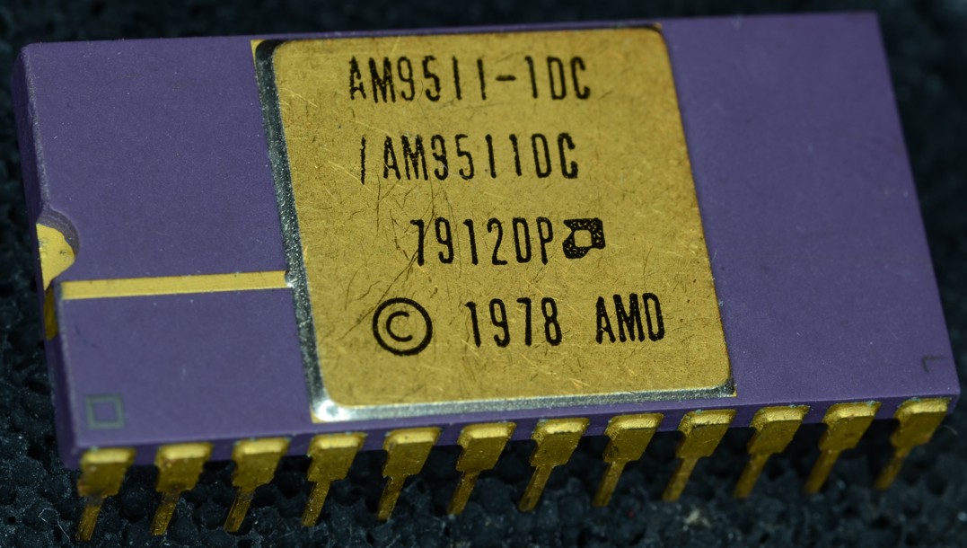
AM9511-1 arithmetic coprocessor

A coprocessor is a computer processor used to supplement the functions of the primary processor (the CPU). Operations performed by the coprocessor may be floating-point arithmetic, graphics, signal processing, string processing, cryptography or I/O interfacing with peripheral devices. By offloading processor-intensive tasks from the main processor, coprocessors can accelerate system performance. Coprocessors allow a line of computers to be customized, so that customers who do not need the extra performance do not need to pay for it.

Functionality

[edit]

Coprocessors vary in their degree of autonomy. Some (such as FPUs) rely on direct control via coprocessor instructions, embedded in the CPU's instruction stream. Others are independent processors in their own right, capable of working asynchronously; they are still not optimized for general-purpose code, or they are incapable of it due to a limited instruction set focused on accelerating specific tasks. It is common for these to be driven by direct memory access (DMA), with the host processor (a CPU) building a command list. The PlayStation 2's Emotion Engine contained an unusual DSP-like SIMD vector unit capable of both modes of operation.

History

[edit]

To make the best use of mainframe computer processor time, input/output tasks were delegated to separate systems called Channel I/O. The mainframe would not require any I/O processing at all, instead, it would set parameters for an input or output operation and then signal the channel processor to carry out the whole of the operation. By dedicating relatively simple sub-processors to handle time-consuming I/O formatting and processing, overall system performance was improved.

Coprocessors for floating-point arithmetic first appeared in desktop computers in the 1970s and became common throughout the 1980s and into the early 1990s. Early 8-bit and 16-bit processors used software to carry out floating-point arithmetic operations. Where a coprocessor was supported, floating-point calculations could be carried out many times faster. Math coprocessors were popular purchases for users of computer-aided design (CAD) software and scientific and engineering calculations. Some floating-point units, such as the AMD 9511, Intel 8231/8232 and Weitek FPUs were treated as peripheral devices, while others such as the Intel 8087, Motorola 68881 and National 32081 were more closely integrated with the CPU.

Another form of coprocessor was a video display coprocessor, as used in the Atari 8-bit computers, TI-99/4A, and MSX home computers, which were called "Video Display Controllers". The Amiga custom chipset includes such a unit known as the Copper, as well as a blitter for accelerating bitmap manipulation in memory.

As microprocessors developed, the cost of integrating the floating-point arithmetic functions into the processor declined. High processor speeds also made a closely integrated coprocessor difficult to implement. Separately packaged mathematics coprocessors are now uncommon in desktop computers. The demand for a dedicated graphics coprocessor has grown, however, particularly due to the increasing demand for realistic 3D graphics in computer games.

Intel

[edit]
i8087 and i80287 microarchitecture
i80387 microarchitecture

The original IBM PC included a socket for the Intel 8087 floating-point coprocessor (aka FPU) which was a popular option for people using the PC for computer-aided design or mathematics-intensive calculations. In that architecture, the coprocessor speeds up floating-point arithmetic on the order of fiftyfold. Users that only used the PC for word processing, for example, saved the high cost of the coprocessor, which would not have accelerated performance of text manipulation operations.

The 8087 was tightly integrated with the 8086/8088 and responded to floating-point machine code operation codes inserted in the 8088 instruction stream. An 8088 processor without an 8087 could not interpret these instructions, requiring separate versions of programs for FPU and non-FPU systems, or at least a test at run time to detect the FPU and select appropriate mathematical library functions.

Intel 80386DX CPU with 80387DX math coprocessor

Another coprocessor for the 8086/8088 central processor was the 8089 input/output coprocessor. It used the same programming technique as 8087 for input/output operations, such as transfer of data from memory to a peripheral device, and so reducing the load on the CPU. But IBM did not use it in IBM PC design and Intel stopped development of this type of coprocessor.

The Intel 80386 microprocessor used an optional "math" coprocessor (the 80387) to perform floating-point operations directly in hardware. The Intel 80486DX processor included floating-point hardware on the chip. Intel released a cost-reduced processor, the 80486SX, that had no floating-point hardware, and also sold an 80487SX coprocessor that essentially disabled the main processor when installed, since the 80487SX was a complete 80486DX with a different set of pin connections.[1]

Intel processors later than the 80486 integrated floating-point hardware on the main processor chip; the advances in integration eliminated the cost advantage of selling the floating-point processor as an optional element. It would be very difficult to adapt circuit-board techniques adequate at 75 MHz processor speed to meet the time-delay, power consumption, and radio-frequency interference standards required at gigahertz-range clock speeds. These on-chip floating-point processors are still referred to as coprocessors because they operate in parallel with the main CPU.

During the era of 8- and 16-bit desktop computers another common source of floating-point coprocessors was Weitek. These coprocessors had a different instruction set from the Intel coprocessors, and used a different socket, which not all motherboards supported. The Weitek processors did not provide transcendental mathematics functions (for example, trigonometric functions) like the Intel x87 family, and required specific software libraries to support their functions.[2]

Motorola

[edit]

The Motorola 68000 family had the 68881/68882 coprocessors which provided similar floating-point speed acceleration as for the Intel processors. Computers using the 68000 family but not equipped with the hardware floating-point processor could trap and emulate the floating-point instructions in software, which, although slower, allowed one binary version of the program to be distributed for both cases. The 68451 memory-management coprocessor was designed to work with the 68020 processor.[3]

Modern coprocessors

[edit]

As of 2001, dedicated Graphics Processing Units (GPUs) in the form of graphics cards are commonplace. Certain models of sound cards have been fitted with dedicated processors providing digital multichannel mixing and real-time DSP effects as early as 1990 to 1994 (the Gravis Ultrasound and Sound Blaster AWE32 being typical examples), while the Sound Blaster Audigy and the Sound Blaster X-Fi are more recent examples.

In 2006, AGEIA announced an add-in card for computers that it called the PhysX PPU. PhysX was designed to perform complex physics computations so that the CPU and GPU do not have to perform these time-consuming calculations. It was designed for video games, although other mathematical uses could theoretically be developed for it. In 2008, Nvidia purchased the company and phased out the PhysX card line; the functionality was added through software allowing their GPUs to render PhysX on cores normally used for graphics processing, using their Nvidia PhysX engine software.

In 2006, BigFoot Systems unveiled a PCI add-in card they christened the KillerNIC which ran its own special Linux kernel on a FreeScale PowerQUICC running at 400 MHz, calling the FreeScale chip a Network Processing Unit or NPU.

The SpursEngine is a media-oriented add-in card with a coprocessor based on the Cell microarchitecture. The SPUs are themselves vector coprocessors.

In 2008, Khronos Group released the OpenCL with the aim to support general-purpose CPUs, ATI/AMD and Nvidia GPUs (and other accelerators) with a single common language for compute kernels.

In 2010s, some mobile computation devices had implemented the sensor hub as a coprocessor. Examples of coprocessors used for handling sensor integration in mobile devices include the Apple M7 and M8 motion coprocessors, the Qualcomm Snapdragon Sensor Core and Qualcomm Hexagon, and the Holographic Processing Unit for the Microsoft HoloLens.

In 2012, Intel announced the Intel Xeon Phi coprocessor.[4]

As of 2016, various companies are developing coprocessors aimed at accelerating artificial neural networks for vision and other cognitive tasks (e.g. vision processing units, TrueNorth, and Zeroth), and as of 2018, such AI chips are in smartphones such as from Apple, and several Android phone vendors.

Other coprocessors

[edit]
  • The MIPS architecture supports up to four coprocessor units, used for memory management, floating-point arithmetic, and two undefined coprocessors for other tasks such as graphics accelerators.[5]
  • Using FPGA (field-programmable gate arrays), custom coprocessors can be created for acceleration of particular processing tasks such as digital signal processing (e.g. Zynq, combines ARM cores with FPGA on a single die).
  • TLS/SSL accelerators, used on servers; such accelerators used to be cards, but in modern times are instructions for crypto in mainstream CPUs.
  • Some multi-core chips can be programmed so that one of their processors is the primary processor, and the other processors are supporting coprocessors.
  • China's Matrix 2000 128 core PCI-e coprocessor is a proprietary accelerator that requires a CPU to run it, and has been employed in an upgrade of the 17,792 node Tianhe-2 supercomputer (2 Intel Knights Bridge+ 2 Matrix 2000 each), now dubbed 2A, roughly doubling its speed at 95 petaflops, exceeding the world's fastest supercomputer.[6]
  • A range of coprocessors were available for various models from Acorn Computers, notably the BBC Micro and BBC Master series. Rather than special-purpose graphics or arithmetic devices, these were general-purpose CPUs (principally the 6502, Zilog Z80, National Semiconductor 32016, and ARM 1) described as second processors, typically interfaced to the host system using a message passing architecture known as the Tube, with Acorn's own products providing such processors in a BBC Micro expansion unit with accompanying memory and interfacing circuitry. Software could be executed independently on the second processor, and applications could be written to offload work from the host system, leaving it to perform input/output tasks, resulting in acceleration. Since a range of CPUs were available in a variety of products, a BBC Micro fitted with such a coprocessor was able to run operating systems for other processor architectures, such as CP/M, DOS and Unix, along with accompanying software.
[edit]

Over time CPUs have tended to grow to absorb the functionality of the most popular coprocessors. FPUs are now considered an integral part of a processors' main pipeline; SIMD units gave multimedia its acceleration, taking over the role of various DSP accelerator cards; and even GPUs have become integrated on CPU dies. Nonetheless, specialized units remain popular away from desktop machines, and for additional power, and allow continued evolution independently of the main processor product lines.

See also

[edit]

References

[edit]
Revisions and contributorsEdit on WikipediaRead on Wikipedia
from Grokipedia
A coprocessor is a specialized computer processor that operates in conjunction with the central processing unit (CPU) to perform specific tasks more efficiently, such as floating-point arithmetic or multimedia processing, often running in parallel with its own control unit.[1] These auxiliary processors can be implemented as separate chips or integrated on the same die as the CPU, communicating via shared buses, dedicated instructions, or memory-mapped interfaces to offload workload from the main processor.[2] The concept of coprocessors emerged in the 1960s with early supercomputers like the CDC 6600, which used dedicated functional units for operations such as multiplication and division to enable parallel execution alongside the CPU.[2] By the 1970s, coprocessors became common in minicomputers and microcomputers, exemplified by the floating-point unit in the DEC PDP-11/45, which handled complex numerical computations independently.[2] A pivotal milestone occurred in 1980 with the introduction of the Intel 8087 math coprocessor, the first dedicated floating-point unit for the x86 architecture, which implemented the IEEE 754 standard for accurate and reliable numerical processing, including 80-bit extended precision and transcendental functions like logarithms.[3] This innovation significantly influenced personal computing, enabling the IBM PC's adoption of Intel processors and setting the foundation for standardized floating-point operations in subsequent hardware.[3] Coprocessors are categorized by their specialized functions, including mathematical units for high-precision calculations, graphics processing units (GPUs) for rendering and parallel computations, and cryptographic accelerators for secure data handling.[4] Other types encompass multimedia coprocessors for streaming acceleration, such as the PipeRench architecture, which uses reconfigurable hardware for efficient video processing via low-latency connections to the CPU. Secure coprocessors, like those in server environments, provide isolated execution for privacy-sensitive applications, allowing dynamic software updates while protecting against tampering.[5] In instruction path coprocessors, programmable on-chip units execute mini-instruction sets to optimize dynamic code paths, enhancing overall system performance.[6] In contemporary computer architecture, coprocessors have evolved from discrete components to tightly integrated elements, such as the floating-point units embedded in modern CPUs and many-core accelerators like GPUs or neural processing units (NPUs), which support high-performance computing tasks including scientific simulations and artificial intelligence workloads.[4] This integration allows for scalable parallelism, as seen in systems where coprocessors handle vectorized media instructions or hardware-accelerated functions, reducing latency and boosting efficiency in domains like artificial intelligence and data analytics.[4] The ongoing development of coprocessors continues to address the growing demands for specialized acceleration in heterogeneous computing environments.[7]

Definition and Functionality

Core Concept

A coprocessor is a specialized auxiliary processor designed to supplement the primary central processing unit (CPU) by performing specific computational tasks that the CPU handles less efficiently, such as complex arithmetic or data-intensive operations.[8] This collaboration enables the coprocessor to execute targeted instructions in parallel with the CPU, thereby enhancing overall system capabilities without requiring the main processor to manage every type of workload.[9] The primary benefits of a coprocessor lie in its ability to offload computationally intensive tasks from the CPU, reducing processing latency, boosting throughput for specialized operations, and facilitating parallel execution that aligns with the coprocessor's optimized architecture rather than the CPU's general-purpose design.[9] By delegating such tasks, the CPU remains free to focus on control flow and other core functions, leading to improved system efficiency in applications requiring high numerical precision or rapid data manipulation.[10] This division of labor is particularly valuable in domains like scientific computing and signal processing, where the coprocessor's dedicated hardware can deliver orders-of-magnitude performance gains over software emulation on the CPU alone.[9] In its basic operational model, a coprocessor interfaces with the CPU through shared buses or dedicated communication channels, monitoring the CPU's instruction stream to identify and execute relevant coprocessor-specific commands while ignoring others.[10] Upon receiving an instruction, the coprocessor fetches operands via the bus, performs independent processing using its own registers and a tailored instruction set—often an extension of the CPU's ISA—and signals completion before returning results for the CPU to integrate into the main execution flow.[9] This synchronized yet autonomous operation ensures seamless data exchange and minimizes synchronization overhead, allowing the system to maintain coherent processing across both units.[2]

Integration with Main Processors

Coprocessors integrate with main processors through various communication protocols that enable efficient data exchange and coordination. Common approaches include shared memory systems, where both the CPU and coprocessor access a common memory space to transfer data without explicit copying, reducing latency in tightly coupled designs.[11] For instance, in heterogeneous systems, data structures are mapped directly to the coprocessor's local memory via a collector mechanism integrated with the CPU's memory controller, preserving original layouts and minimizing overhead.[11] Dedicated buses, such as local coprocessor interface buses, provide a direct, high-speed pathway for instruction and data transfer, often synchronized with the CPU's clock to support real-time operation in system-on-chip (SoC) environments.[12] Interrupt signals further facilitate asynchronous communication, allowing the coprocessor to notify the CPU of task completion or errors, ensuring seamless workflow in multi-component systems.[13] Instruction handling between the CPU and coprocessor typically involves the CPU issuing specialized opcodes that the coprocessor recognizes and executes. In architectures like x86, escape (ESC) instructions occupy a dedicated opcode range (e.g., D8 to DF), which the CPU passes to the coprocessor for decoding and processing while handling memory address computations itself.[3] The coprocessor traps these opcodes, executes the corresponding operations—such as floating-point arithmetic—and signals readiness for the next instruction, allowing the CPU to either wait idly or proceed with independent tasks to optimize overall throughput.[3] This mechanism ensures that coprocessor-specific computations are offloaded transparently, with the CPU maintaining control over the instruction stream by snooping the bus or prefetch queue.[14] Synchronization methods are essential to maintain data integrity and coordinate execution between the CPU and coprocessor. Busy-wait polling, where the CPU repeatedly checks a status flag until the coprocessor completes its task, provides simple but resource-intensive synchronization, often used in low-latency scenarios.[13] Handshaking signals, such as request/grant (RQ/GT) pins, enable more efficient immediate synchronization by allowing the coprocessor to seize bus control temporarily, preventing conflicts during memory accesses without requiring explicit waits.[14] Event-driven interrupts offer asynchronous coordination, where the coprocessor asserts an interrupt upon finishing, prompting the CPU to resume dependent operations; this approach minimizes idle time and supports interruptible busy-waiting to handle higher-priority events.[13] In practice, combinations of these methods, like the BUSY signal in early designs, ensure the CPU pauses only when necessary, tracking coprocessor state to avoid race conditions.[14] Coprocessors typically share the main processor's power supply and memory hierarchy to form a cohesive system unit, with integrated voltage regulation and adaptive clocking managing overall consumption in modern SoCs. This sharing extends to thermal management, where coprocessors contribute to on-chip power density, necessitating system-level techniques like dynamic throttling to distribute heat and prevent hotspots across the die.[15] Bandwidth allocation in the shared memory hierarchy prioritizes data flows, often using hybrid cache policies to balance access efficiency between CPU and coprocessor tasks, ensuring sustained performance without excessive contention.[11]

Historical Development

Early Innovations (1970s–1980s)

Before the emergence of microprocessor-based coprocessors, mainframe systems incorporated specialized hardware for floating-point arithmetic as analogous concepts to accelerate numerical computations. The IBM System/360 family, announced in 1964, offered optional floating-point features that supported both short (32-bit) and long (64-bit) precision operations, significantly enhancing the speed and efficiency of scientific and engineering calculations on its integrated processing units.[16] These capabilities demonstrated the value of dedicated arithmetic hardware to handle tasks beyond the core integer processing of early computers, setting the stage for discrete coprocessors in microcomputer architectures. Coprocessors as separate chips emerged in the late 1970s, with early examples like AMD's Am9511 arithmetic processing unit introduced in 1977 for microprocessors such as the Intel 8080. For the x86 architecture, Intel's 8087 Numeric Data Processor, released in 1980, became a seminal example, designed specifically to complement the 8086 microprocessor by offloading floating-point operations.[3] This coprocessor supported 80-bit extended precision for internal temporaries, allowing for greater accuracy in real-number arithmetic compared to the 8086's 16-bit integer focus, and it implemented a stack-based register architecture with eight 80-bit registers.[17] A key innovation of the 8087 was its hardware support for transcendental functions, including sine, cosine, tangent, arctangent, logarithm, and exponential operations, which were computed using algorithms like CORDIC for efficiency.[17] Operating at clock speeds up to 5 MHz in its standard variant—synchronized with the host CPU—the 8087 executed floating-point additions, multiplications, divisions, and square roots at rates far exceeding software emulation, thereby minimizing CPU overhead for math-intensive tasks.[3][17] The adoption of early coprocessors like the 8087 was propelled by the inherent limitations of integer-only microprocessors such as the 8086, which struggled with decimal, floating-point, and vector mathematics required in engineering simulations, scientific modeling, and data processing.[3] By enabling high-speed FLOPs and precise arithmetic, the 8087 addressed these gaps, fostering broader use of microcomputers in technical applications and influencing the development of standardized numerical computing practices.[3]

Advancements in the 1990s

The Intel 80287, introduced as a successor to the 8087, served as the numeric coprocessor for the 80286 microprocessor, offering enhanced compatibility through shared bus architecture and synchronized operation modes.[18] It supported clock speeds ranging from 5 MHz to 12 MHz, enabling more efficient handling of floating-point operations in systems like the IBM PC/AT derivatives.[19] The 80387 further advanced this lineage for the 80386 CPU, achieving clock speeds up to 25 MHz in standard configurations and incorporating parallel functional units for improved throughput, including support for pipelined bus cycles that reduced latency in data transfers.[20] These coprocessors maintained full backward compatibility with earlier x87 designs while extending the instruction set to include over 70 numeric operations, facilitating seamless upgrades in 32-bit protected mode environments.[20] During the 1990s, coprocessor technology began transitioning from discrete components toward on-chip integration, driven by the need for reduced latency and simplified system design. Early experiments involved embedding floating-point units (FPUs) directly onto the main processor die, with Intel's Pentium microprocessor—launched in 1993—marking a pivotal milestone by incorporating a fully integrated FPU capable of superscalar execution.[21] This integration eliminated the requirement for separate coprocessor chips like the 80387, cutting costs and improving performance by allowing simultaneous integer and floating-point operations, with the FPU pipeline handling one floating-point instruction per clock cycle.[22] Subsequent Pentium variants refined this approach, boosting overall system efficiency and paving the way for broader adoption in personal computing. Performance advancements in 1990s coprocessors were quantified through metrics like MFLOPS, with the 80387 achieving around 0.3 MFLOPS in typical double-precision workloads at 25 MHz on Linpack benchmarks, a significant leap that supported real-time simulations in scientific and engineering applications.[23] This throughput, derived from optimized execution of basic arithmetic instructions (e.g., add and multiply taking 10–30 cycles), enabled practical use in fields like computer-aided design, where prior discrete designs struggled with bottlenecks. MIPS ratings for coprocessor-specific instructions also improved, reflecting pipelined enhancements that increased effective instructions per second by up to 20% over the 80287.[20] These developments profoundly influenced software ecosystems, as compilers began incorporating optimizations tailored to coprocessor presence. For instance, Microsoft C/C++ version 6.0 (1989, with updates through the 1990s) provided flags like /FPc87 to generate code assuming an 80x87-series coprocessor, enabling intrinsic functions for direct FPU access and accelerating floating-point computations in applications.[24] Such tools encouraged developers to leverage coprocessor capabilities, fostering growth in numerically intensive software for Windows platforms and reducing reliance on software emulation.

Key Manufacturers and Examples

Intel Implementations

Intel's coprocessor lineup began with the 8087 Numeric Data Processor, introduced in 1980 as the first floating-point coprocessor for the 8086 microprocessor, featuring 40,000 transistors and capable of approximately 50,000 floating-point operations per second (0.05 MFLOPS).[25] Designed in HMOS technology with a 40-pin package, it extended the 8086's capabilities for scientific and engineering applications by handling complex arithmetic independently.[26] This was followed by the 80287 in 1982, a high-performance extension for the 80286, built on HMOS III technology in a 40-pin ceramic DIP package, supporting integer, floating-point, and BCD formats while maintaining object-code compatibility with the 8087.[18] The 80387, released in 1987 for the 80386, advanced the series with full compliance to the IEEE 754 standard, including support for denormals, NaNs, and rounding modes, in a 68-pin grid array package operating synchronously with the host CPU.[27] Complementing these x87 math coprocessors, Intel introduced the i860 in 1989, a 64-bit RISC microprocessor with over 1 million transistors, optimized for vector processing in supercomputing environments through pipelined floating-point units achieving up to 80 MFLOPS in single precision at 40 MHz.[28] The x87 family, encompassing the 8087, 80287, and 80387, employed a stack-based register architecture with eight 80-bit registers organized as a last-in, first-out (LIFO) structure, where operations reference positions relative to the top-of-stack (ST(0)) pointer in the status word.[27] This model supported extended precision (64-bit mantissa) for internal computations, alongside single (32-bit), double (64-bit), and packed BCD formats, enabling precise handling of transcendental functions like sine and logarithm while adhering to IEEE 754 for arithmetic accuracy, including gradual underflow and exception flags for invalid operations, overflow, and inexact results.[27] The architecture integrated seamlessly via ESCAPE instructions, allowing the coprocessor to execute in parallel with the main CPU without halting the system bus.[29] Compatibility was a core design principle, with pin-compatible variants like the 80387DX for the 80386DX and 80387SX for the 80386SX, enabling straightforward upgrades within the 386 family via the dedicated math coprocessor socket.[27] The 80387 preserved full object-code compatibility with 8087 and 80287 software, running existing programs unchanged in real-address mode and supporting virtual-8086 mode for multitasking, though it introduced refinements such as distinct signaling for NaNs absent in prior models.[27] This backward compatibility extended to earlier CPUs like the 80286 through shared sockets in some systems, facilitating incremental enhancements without redesigning motherboards or rewriting code. By the mid-1990s, Intel's coprocessors had achieved widespread adoption, powering personal computers through their integration as standard components in x86 systems and contributing to Intel's dominance in the microprocessor market. This prevalence drove the evolution toward software-emulated alternatives, exemplified by the MMX instruction set extensions introduced in 1996, which repurposed existing registers for multimedia vector operations, bridging the gap to fully integrated floating-point units in later CPUs.[30]

Motorola and Other Early Designs

The Motorola 68881 and 68882 floating-point coprocessors, introduced in the 1980s, served as dedicated arithmetic units for the MC68020 and MC68030 microprocessors in the 68000 family.[31] These devices extended the host CPU's capabilities by handling IEEE 754-compliant floating-point operations, including addition, multiplication, division, and transcendental functions like sine and logarithm, all performed internally at 80-bit extended precision (64-bit mantissa and 15-bit exponent) using a 67-bit arithmetic unit and barrel shifter.[32] The 68881 featured a basic architecture divided into a Bus Interface Unit (BIU) for communication and an Arithmetic Processing Unit (APU) for execution, while the 68882 improved upon this with dual-ported registers, an added Conversion Unit (CU), and enhanced concurrency, achieving over twice the performance of its predecessor through parallel instruction handling.[33] Both supported eight 80-bit floating-point data registers (FP0–FP7) and three 32-bit control registers for status, precision control, and instruction addressing.[31] Architecturally, these coprocessors integrated via the M68000 family's coprocessor interface, which allowed up to eight such devices per system and used standard asynchronous bus cycles for data transfer.[32] A key feature was support for dynamic bus sizing, enabling seamless operation over 8-, 16-, or 32-bit data buses without additional glue logic, which provided flexibility in system design compared to more rigid interfaces in contemporary x86 alternatives.[33] The 68881 employed a sequential execution model where the host CPU waited for APU availability, but the 68882 introduced pipelining across the BIU, CU, and APU to overlap instruction fetch, decode, and execution, supporting clock speeds up to 33 MHz (with later variants reaching 40 MHz).[31] This design emphasized high-precision computation for scientific and engineering applications, with all operations rounded to at most one unit in the last place (ulp) for accuracy up to 19 decimal digits.[32] These coprocessors found adoption in niche ecosystems outside the dominant x86 market, particularly in Apple's Macintosh II series and Commodore's Amiga 3000 workstations, where they accelerated graphics, simulations, and CAD tasks. By 1990, systems using 68000-based architectures like those from Apple and Commodore held a significant share of alternative computing platforms.[34] Other early vendors offered alternatives to Intel's dominance in x86 coprocessors. AMD produced the Am287 and Am387 as pin- and software-compatible equivalents to the Intel 80287 and 80387, respectively, providing second-sourcing for floating-point acceleration in 286 and 386 systems with similar 80-bit register stacks and IEEE 754 support, but at potentially lower cost for OEMs.[35] Meanwhile, Cyrix produced compatible coprocessors like the 387, offering similar functionality at lower cost for 386 systems. Weitek's WTL 3167 targeted high-speed vector mathematics in professional workstations paired with the Intel 80386, delivering 2-3 times the performance of the 80387 through a pipelined architecture optimized for single- and double-precision operations in scientific computing and graphics rendering.[36] These designs contrasted with Motorola's by focusing on x86 compatibility and vector extensions, yet shared the goal of offloading complex math from the main CPU to enable embedded and workstation applications in the late 1980s.[36]

Modern Coprocessors

Graphics and Compute Accelerators

Graphics processing units (GPUs) have evolved into versatile coprocessors, extending beyond visual rendering to general-purpose computing on graphics processing units (GPGPU). NVIDIA's Compute Unified Device Architecture (CUDA), introduced in 2006, marked a pivotal advancement by enabling developers to program GPUs for non-graphics workloads such as scientific simulations and data processing.[37] Similarly, AMD's Stream SDK, launched around 2008 as part of the FireStream initiative, facilitated stream processing on Radeon-based hardware, allowing parallel execution of compute-intensive tasks.[38] These frameworks leverage the GPU's architecture, which incorporates thousands of simpler cores optimized for single instruction, multiple data (SIMD) operations, enabling massive parallelism for tasks that benefit from concurrent thread execution.[39] Key to their efficacy as coprocessors are features that streamline integration with host CPUs. NVIDIA's Unified Virtual Addressing (UVA), introduced in CUDA 4.0, establishes a single virtual address space across CPU and GPU memory, simplifying data sharing and pointer manipulation without explicit copies.[40] Complementing this, the OpenCL (Open Computing Language) API, developed by the Khronos Group, provides a cross-vendor standard for orchestrating heterogeneous computing, allowing kernels to run on diverse accelerators including GPUs while abstracting hardware differences.[41] These mechanisms enable seamless CPU-GPU collaboration, where the CPU handles sequential control flow and the GPU accelerates vectorized computations. Modern GPUs in the NVIDIA GeForce RTX 50 series (as of 2025) exemplify high-performance coprocessing, with the flagship RTX 5090 delivering 104.8 teraflops (TFLOPS) in single-precision floating-point (FP32) operations, significantly offloading complex workloads like real-time ray tracing and AI inference from the CPU.[42] This capability stems from architectures with up to 21,760 CUDA cores, which process graphics pipelines and compute shaders in parallel. In applications such as scientific computing, GPUs accelerate molecular dynamics simulations by performing force calculations on vast particle sets, achieving speedups of orders of magnitude over CPU-only implementations due to their parallel throughput.[43] Likewise, in cryptocurrency mining—particularly for algorithms like Ethash—GPUs outperform CPUs by factors of 10 to 100 times, as their numerous arithmetic units efficiently hash parallel data streams.[44]

Specialized Domain Accelerators

Specialized domain accelerators represent coprocessors designed for specific, high-performance workloads in fields like networking, security, and artificial intelligence, offloading tasks from general-purpose CPUs to achieve superior efficiency and throughput. These devices leverage custom architectures to handle domain-specific operations, such as packet manipulation in networking or tensor computations in AI, enabling scalable performance in data centers and edge systems. Network Processing Units (NPUs) exemplify this specialization, with Broadcom's Jericho series providing programmable packet processors capable of terabit-scale routing. For instance, the Jericho2 (BCM88690) delivers 9.6 Tb/s of packet processing capacity, supporting up to twelve 400 GbE ports while integrating accelerators for tasks like checksum calculations and Quality of Service (QoS) enforcement.[45] These features allow the NPU to perform on-the-fly modifications, including UDP checksum updates and CRC computations, without CPU involvement, ensuring low-latency handling of ingress and egress traffic in high-density Ethernet fabrics.[46] Similarly, the Jericho3 extends this to 28.8 Tb/s with deep buffering and hierarchical QoS scheduling, optimizing for congestion management in carrier-grade networks.[47] By distributing scheduling across packet buffers, Jericho NPUs maintain state-of-the-art traffic prioritization, reducing jitter for real-time applications like video streaming or VoIP.[48] Cryptographic coprocessors further illustrate domain-specific acceleration, particularly for secure data handling. IBM's PCIe Cryptographic Coprocessors, operating under the Common Cryptographic Architecture (CCA), provide hardware-accelerated key management and encryption services compliant with standards like FIPS 140-2 Level 4.[49] These devices support AES encryption at high speeds, enabling secure storage and processing of sensitive keys without exposing them to the host system.[50] The 4769 model, for example, integrates multiple AES engines per coprocessor, facilitating operations like data encryption and digital signing in enterprise environments such as financial transactions or cloud security.[50] This offload minimizes latency for bulk encryption workloads, with battery-backed memory ensuring key persistence during power events. In artificial intelligence, Google's Tensor Processing Unit (TPU), introduced in 2015, serves as a pioneering AI accelerator optimized for deep learning inference. The TPU employs a systolic array architecture—a 256×256 grid of 65,536 multiply-accumulate units—for efficient matrix multiplications central to tensor operations in neural networks.[51] This design processes 8-bit integer operations at 92 tera-operations per second (TOPS), tailored for convolutions and fully connected layers in models like those used for image recognition.[52] Unlike general-purpose GPUs, the TPU's focus on inference yields significantly higher efficiency, achieving 15–30 times the performance and 30–80 times the performance-per-watt of contemporary CPUs and GPUs for neural network tasks.[52] Later iterations build on this, such as the 2025 Ironwood TPU, which delivers over 100 TOPS per watt in inference scenarios through architectural improvements like 2x perf/watt gains over predecessors, underscoring their advantage in power-constrained deployments over broader but less specialized GPU coverage.[53][54]

Integration in System-on-Chips

In system-on-chip (SoC) architectures, coprocessors such as neural processing units (NPUs) and graphics processing units (GPUs) are tightly integrated onto a single die alongside central processing units (CPUs), enabling seamless data sharing and minimized inter-component communication delays. For instance, Apple's A-series chips, like the A16 Bionic, embed a 16-core Neural Engine and multi-core GPU within the same silicon, allowing unified memory access that reduces latency for AI and graphics tasks by eliminating off-chip data transfers.[55] This monolithic approach contrasts with discrete designs, fostering efficient resource allocation in mobile and embedded systems where space and speed are paramount. The benefits of such integrated designs stem from the elimination of external interfaces, leading to substantial reductions in power consumption and enhancements in data throughput. Mobile SoCs typically operate within a 5–10 W envelope, where on-chip coprocessor integration cuts energy use by avoiding the overhead of board-level signaling, as seen in ARM-based platforms.[56] Furthermore, interconnects like ARM's CoreLink Coherent Interconnect (CCI-550) provide high-bandwidth pathways—supporting up to six coherent interfaces with 2x snoop efficiency—facilitating rapid data exchange between heterogeneous cores while maintaining cache coherency and low power overhead.[57] A prominent case study is Qualcomm's Snapdragon series, where the Hexagon DSP serves as an integrated coprocessor for audio processing, offloading tasks from the CPU to achieve up to 32x performance efficiency over general-purpose software implementations.[58] In devices like smartphones, this enables real-time audio enhancement with minimal battery drain, as the DSP handles voice and signal processing directly via streaming modes that bypass main memory, improving overall system responsiveness. Despite these advantages, integrating coprocessors into dense SoCs introduces challenges, particularly in thermal management and software development. High-performance heterogeneous cores generate concentrated heat, complicating dissipation in compact form factors and risking thermal throttling or reliability issues under sustained loads.[59] Additionally, the diverse instruction sets of specialized accelerators versus general CPUs create programmability trade-offs, requiring complex tools for workload partitioning and optimization to fully leverage the architecture without excessive developer overhead.[60]

Future Directions in AI and Edge Computing

The evolution of coprocessors in AI is increasingly driven by neuromorphic designs that emulate biological neural processes for efficient, sparse computing. Intel's Loihi, introduced in 2017, represents a seminal example, featuring 128 neuromorphic cores that mimic brain synapses through spiking neural networks and on-chip learning capabilities, enabling asynchronous, event-driven computation with minimal energy use suitable for edge inference tasks.[61][62] Subsequent iterations, such as Loihi 2, further optimize for sparse activity and reduced data movement, targeting applications in robotics and sensor processing where power constraints are critical.[63] In edge computing, coprocessors are poised to enable real-time analytics in resource-constrained environments, particularly within the burgeoning Internet of Things (IoT) ecosystem. Projections indicate that the number of connected IoT devices will reach approximately 40 to 50 billion by 2030, necessitating on-device processing to handle latency-sensitive tasks like anomaly detection and predictive maintenance without relying on cloud infrastructure.[64][65] Coprocessors integrated into these devices, such as dedicated AI accelerators, will facilitate efficient execution of machine learning models directly at the edge, reducing bandwidth demands and enhancing privacy.[66] Looking ahead, technological advancements in coprocessors include hybrid quantum-classical systems and advanced packaging techniques to achieve unprecedented performance in compact formats. IBM's Qiskit framework supports extensions for hybrid workflows, where quantum processors act as coprocessors alongside classical hardware to tackle optimization and simulation problems intractable for traditional systems.[67] Complementing this, 3D-stacked designs are emerging to deliver over 1 petaFLOPS of compute in small-form-factor devices, as demonstrated by prototypes like NVIDIA's DGX Spark, which leverages layered integration for high-density AI acceleration while improving energy efficiency.[68][69] Industry forecasts underscore the growing dominance of coprocessors in AI workloads, with a strong emphasis on sustainability. By 2029, more than 65% of spending on AI-optimized infrastructure as a service (IaaS) is expected to focus on inference tasks, where specialized coprocessors play a central role in scaling deployments efficiently.[70] This shift aligns with broader goals to mitigate AI's energy footprint, as energy-efficient computing emerges as a top trend, potentially reducing data center power demands amid rising sustainability pressures.[71]

References

User Avatar
No comments yet.