Hubbry Logo
Magnetic-core memoryMagnetic-core memoryMain
Open search
Magnetic-core memory
Community hub
Magnetic-core memory
logo
8 pages, 0 posts
0 subscribers
Be the first to start a discussion here.
Contribute something
Magnetic-core memory
from Wikipedia

A 32 × 32 core memory plane storing 1024 bits (or 128 bytes) of data. The small black rings at the intersections of the grid wires, organised in four squares, are the ferrite cores.

In computing, magnetic-core memory is a form of random-access memory. It predominated for roughly 20 years between 1955 and 1975, and is often just called core memory, or, informally, core.

Core memory uses toroids (rings) of a hard magnetic material (usually a semi-hard ferrite). Each core stores one bit of information. Two or more wires pass through each core, forming an X-Y array of cores. When an electrical current above a certain threshold is applied to the wires, the core will become magnetized. The core to be assigned a value – or written – is selected by powering one X and one Y wire to half of the required current, such that only the single core at the intersection is written. Depending on the direction of the currents, the core will pick up a clockwise or counterclockwise magnetic field, storing a 1 or 0.

This writing process also causes electricity to be induced into nearby wires. If the new pulse being applied in the X-Y wires is the same as the last applied to that core, the existing field will do nothing, and no induction will result. If the new pulse is in the opposite direction, a pulse will be generated. This is normally picked up in a separate "sense" wire, allowing the system to know whether that core held a 1 or 0. As this readout process requires the core to be written, this process is known as destructive readout, and requires additional circuitry to reset the core to its original value if the process flipped it.

When not being read or written, the cores maintain the last value they had, even if the power is turned off. Therefore, they are a type of non-volatile memory. Depending on how it was wired, core memory could be exceptionally reliable. Read-only core rope memory, for example, was used on the mission-critical Apollo Guidance Computer essential to NASA's successful Moon landings.[1]

Using smaller cores and wires, the memory density of core slowly increased. By the late 1960s a density of about 32 kilobits per cubic foot (about 0.9 kilobits per litre)[citation needed] was typical. The cost declined over this period from about $1 per bit to about 1 cent per bit. Reaching this density requires extremely careful manufacturing, which was almost always carried out by hand in spite of repeated major efforts to automate the process. Core was almost universal until the introduction of the first semiconductor memory chips in the late 1960s, and especially dynamic random-access memory (DRAM) in the early 1970s. Initially around the same price as core, DRAM was smaller and simpler to use. Core was driven from the market gradually between 1973 and 1978.

Even after magnetic-core memory became obsolete with semiconductors, main memory was often still referred to as "core", particularly by people used to the term who worked on older machines with magnetic-core memory. The process of copying the entire content of a computer's main memory to a disk file for further inspection by a system programmer is still called a "core dump". When core memory used for calculations was expensive and a scarce resource, technologies were developed to swap blocks of data "out of core" onto larger, slower storage. Algorithms whose working set size exceeds main memory came to be called out-of-core algorithms, while in-core algorithms fit in main memory.

History

[edit]

Developers

[edit]
Project Whirlwind core memory

The basic concept of using the square hysteresis loop of certain magnetic materials as a storage or switching device was known from the earliest days of computer development. Much of this knowledge had developed due to an understanding of transformers, which allowed amplification and switch-like performance when built using certain materials. The stable switching behavior was well known in the electrical engineering field, and its application in computer systems was immediate. For example, J. Presper Eckert and Jeffrey Chuan Chu had done some development work on the concept in 1945 at the Moore School during the ENIAC efforts.[2]

Robotics pioneer George Devol filed a patent[3] for the first static (non-moving) magnetic memory on 3 April 1946. Devol's magnetic memory was further refined via 5 additional patents[4][5][6][7][8] and ultimately used in the first industrial robot. Frederick Viehe applied for various patents on the use of transformers for building digital logic circuits in place of relay logic beginning in 1947. A fully developed core system was patented in 1947, and later purchased by IBM in 1956.[9] This development was little-known, however, and the mainstream development of core memory is normally associated with three independent teams.

Substantial work in the field was carried out by the Shanghai-born American physicists An Wang and Way-Dong Woo, who created the pulse transfer controlling device in 1949.[10] The patent described a type of memory that would today be known as a delay-line or shift-register system. Each bit was stored using a pair of transformers, one that held the value and a second used for control. A signal generator produced a series of pulses that were sent into the control transformers at half the energy needed to flip the polarity. The pulses were timed so the field in the transformers had not faded away before the next pulse arrived. If the storage transformer's field matched the field created by the pulse, then the total energy would cause a pulse to be injected into the next transformer pair. Those that did not contain a value simply faded out. Stored values were thus moved bit by bit down the chain with every pulse. Values were read out at the end, and fed back into the start of the chain to keep the values continually cycling through the system.[11] Such systems have the disadvantage of not being random-access, to read any particular value one has to wait for it to cycle through the chain. Wang and Woo were working at Harvard University's Computation Laboratory at the time, and the university was not interested in promoting inventions created in their labs. Wang was able to patent the system on his own.

The MIT Project Whirlwind computer required a fast memory system for real-time aircraft tracking. At first, an array of Williams tubes—a storage system based on cathode-ray tubes—was used, but proved temperamental and unreliable. Several researchers in the late 1940s conceived the idea of using magnetic cores for computer memory, but MIT computer engineer Jay Forrester received the principal patent for his invention of the coincident-current core memory that enabled the 3D storage of information.[12][13] William Papian of Project Whirlwind cited one of these efforts, Harvard's "Static Magnetic Delay Line", in an internal memo. The first core memory of 32 × 32 × 16 bits was installed on Whirlwind in the summer of 1953. Papian stated: "Magnetic-Core Storage has two big advantages: (1) greater reliability with a consequent reduction in maintenance time devoted to storage; (2) shorter access time (core access time is 9 microseconds: tube access time is approximately 25 microseconds) thus increasing the speed of computer operation."[14]

In April 2011, Forrester recalled, "the Wang use of cores did not have any influence on my development of random-access memory. The Wang memory was expensive and complicated. As I recall, which may not be entirely correct, it used two cores per binary bit and was essentially a delay line that moved a bit forward. To the extent that I may have focused on it, the approach was not suitable for our purposes." He describes the invention and associated events, in 1975.[15] Forrester has since observed, "It took us about seven years to convince the industry that random-access magnetic-core memory was the solution to a missing link in computer technology. Then we spent the following seven years in the patent courts convincing them that they had not all thought of it first."[16]

A third developer involved in the early development of core memory was Jan A. Rajchman at RCA. A prolific inventor, Rajchman designed a unique core system using ferrite bands wrapped around thin metal tubes,[17] building his first examples using a converted aspirin press in 1949.[9] Rajchman later developed versions of the Williams tube and led the development of the Selectron.[18]

Two key inventions led to the development of magnetic core memory in 1951. The first, An Wang's, was the write-after-read cycle, which solved the problem of how to use a storage medium in which the act of reading erased the data read, enabling the construction of a serial, one-dimensional shift register (of 50 bits), using two cores to store a bit. A Wang core shift register is in the Revolution exhibit at the Computer History Museum. The second, Forrester's, was the coincident-current system, which enabled a small number of wires to control a large number of cores enabling 3D memory arrays of several million bits. The first use of magnetic core was in the Whirlwind computer,[19] and Project Whirlwind's "most famous contribution was the random-access, magnetic core storage feature."[20] Commercialization followed quickly. Magnetic core was used in peripherals of the ENIAC in 1953,[21] the IBM 702[22] delivered in July 1955, and later in the 702 itself. The IBM 704 (1954) and the Ferranti Mercury (1957) used magnetic-core memory.

It was during the early 1950s that Seeburg Corporation developed one of the first commercial applications of coincident-current core memory storage in the "Tormat" memory of its new range of jukeboxes, starting with the V200 developed in 1953 and released in 1955.[23] Numerous uses in computing, telephony and industrial process control followed.

Patent disputes

[edit]

Wang's patent was not granted until 1955, and by that time magnetic-core memory was already in use. This started a long series of lawsuits, which eventually ended when IBM bought the patent outright from Wang for US$500,000.[24] Wang used the funds to greatly expand Wang Laboratories, which he had co-founded with Dr. Ge-Yao Chu, a schoolmate from China.

MIT wanted to charge IBM $0.02 per bit royalty on core memory. In 1964, after years of legal wrangling, IBM paid MIT $13 million for rights to Forrester's patent—the largest patent settlement to that date.[25][26]

Production economics

[edit]

In 1953, tested but not-yet-strung cores cost US$0.33 each. As manufacturing volume increased, by 1970 IBM was producing 20 billion cores per year, and the price per core fell to US$0.0003. Core sizes shrank over the same period from around 0.1 inches (2.5 mm) diameter in the 1950s to 0.013 inches (0.33 mm) in 1966.[27] The power required to flip the magnetization of one core is proportional to the volume, so this represents a drop in power consumption by a factor of 125.

The cost of complete core memory systems was dominated by the cost of stringing the wires through the cores. Forrester's coincident-current system required one of the wires to be run at 45 degrees to the cores, which proved difficult to wire by machine, so that core arrays had to be assembled under microscopes by workers with fine motor control.

In 1956, a group at IBM filed for a patent on a machine to automatically thread the first few wires through each core. This machine held the full plane of cores in a "nest" and then pushed an array of hollow needles through the cores to guide the wires.[28] Use of this machine reduced the time taken to thread the straight X and Y select lines from 25 hours to 12 minutes on a 128 by 128 core array.[29]

Smaller cores made the use of hollow needles impractical, but there were numerous advances in semi-automatic core threading. Support nests with guide channels were developed. Cores were permanently bonded to a backing sheet "patch" that supported them during manufacture and later use. Threading needles were butt welded to the wires, the needle and wire diameters were the same, and efforts were made to eliminate the use of needles.[30][31]

The most important change, from the point of view of automation, was the combination of the sense and inhibit wires, eliminating the need for a circuitous diagonal sense wire. With small changes in layout, this also allowed much tighter packing of the cores in each patch.[32][33]

By the early 1960s, the cost of core fell to the point that it became nearly universal as main memory, replacing both inexpensive low-performance drum memory and costly high-performance systems using vacuum tubes, and later discrete transistors as memory. The cost of core memory declined sharply over the lifetime of the technology: costs began at roughly US$1.00 per bit and dropped to roughly US$0.01 per bit.

Core memory was made obsolete by semiconductor integrated circuit memories in the 1970s, though remained in use for mission-critical and high-reliability applications in the IBM System/4 Pi AP-101 (used in the Space Shuttle until an upgrade in early 1990s, and the B-52 and B-1B bombers).[34][35][36]

An example of the scale, economics, and technology of core memory in the 1960s was the 256K 36-bit word (1.2 MiB[a]) core memory unit installed on the PDP-6 at the MIT Artificial Intelligence Laboratory by 1967.[37] This was considered "unimaginably huge" at the time, and nicknamed the "Moby Memory".[38] It cost $380,000 ($0.04/bit) and its width, height and depth was 175 cm × 127 cm × 64 cm (69 in × 50 in × 25 in) with its supporting circuitry (189 kilobits/cubic foot = 6.7 kilobits/litre). Its cycle time was 2.75 μs.[39][40][41]

In 1980, the price of a 16 kW (kiloword, equivalent to 32 kB) core memory board that fitted into a DEC Q-bus computer was around US$3,000. At that time, core array and supporting electronics could fit on a single printed circuit board about 25 cm × 20 cm (10 in × 8 in) in size, the core array was mounted a few mm above the PCB and was protected with a metal or plastic plate.[citation needed]

Description

[edit]
Diagram of a 4×4 plane of magnetic core memory in an X/Y line coincident-current setup. X and Y are drive lines, S is sense, Z is inhibit. Arrows indicate the direction of current for writing.
Close-up of a core plane. The distance between the rings is roughly 1 mm (0.04 in). The green horizontal wires are X; the Y wires are dull brown and vertical, toward the back. The sense wires are diagonal, colored orange, and the inhibit wires are vertical twisted pairs.

The term "core" comes from conventional transformers whose windings surround a magnetic core. In core memory, the wires pass once through any given core—they are single-turn devices. The properties of materials used for memory cores are dramatically different from those used in power transformers. The magnetic material for a core memory requires a high degree of magnetic remanence, the ability to stay highly magnetized, and a low coercivity so that less energy is required to change the magnetization direction. The core can take two states, encoding one bit. Core memory contents are retained even when the memory system is powered down (non-volatile memory). However, when the core is read, it is reset to a "zero" value. Circuits in the computer memory system then restore the information in an immediate re-write cycle.

How core memory works

[edit]
One of three inter-connected modules that make up an Omnibus-based (PDP 8/e/f/m) PDP-8 core memory plane
One of three inter-connected modules that make up an Omnibus-based PDP-8 core memory plane. This is the middle of the three and contains the array of actual ferrite cores.
One of three inter-connected modules that make up an Omnibus-based PDP-8 core memory plane

The most common form of core memory, X/Y line coincident-current, used for the main memory of a computer, consists of a large number of small toroidal ferrimagnetic ceramic ferrites (cores) held together in a grid structure (organized as a "stack" of layers called planes), with wires woven through the holes in the cores' centers. In early systems there were four wires: X, Y, Sense, and Inhibit, but later cores combined the latter two wires into one Sense/Inhibit line.[32] Each toroid stored one bit (0 or 1). One bit in each plane could be accessed in one cycle, so each machine word in an array of words was spread over a "stack" of planes. Each plane would manipulate one bit of a word in parallel, allowing the full word to be read or written in one cycle.

Core relies on the square hysteresis loop properties of the ferrite material used to make the toroids. An electric current in a wire that passes through a core creates a magnetic field. Only a magnetic field greater than a certain intensity ("select") can cause the core to change its magnetic polarity. To select a memory location, one of the X and one of the Y lines are driven with half the current ("half-select") required to cause this change. Only the combined magnetic field generated where the X and Y lines cross (the logical conjunction) is sufficient to change the state; other cores will see only half the needed field ("half-selected"), or none at all. By driving the current through the wires in a particular direction, the resulting induced field forces the selected core's magnetic flux to circulate in one direction or the other (clockwise or counterclockwise). One direction is a stored 1, while the other is a stored 0.

The toroidal shape of a core is preferred since the magnetic path is closed, there are no magnetic poles and thus very little external flux. This allows the cores to be packed closely together without their magnetic fields interacting. The alternating 45-degree positioning used in early core arrays was necessitated by the diagonal sense wires. With the elimination of these diagonal wires, tighter packing was possible.[33]

Reading and writing

[edit]
Diagram of the hysteresis curve for a magnetic memory core during a read operation. Sense line current pulse is high ("1") or low ("0") depending on original magnetization state of the core.

The access time plus the time to rewrite is the memory cycle time.

Reading

[edit]

To read a bit of core memory, the circuitry tries to flip the bit to the polarity assigned to the 0 state, by driving the selected X and Y lines that intersect at that core.

  • If the bit was already 0, the physical state of the core is unaffected.
  • If the bit was previously 1, then the core changes magnetic polarity. This change, after a delay, induces a voltage pulse into the Sense line.

The detection of such a pulse means that the bit had most recently contained a 1. Absence of the pulse means that the bit had contained a 0. The delay in sensing the voltage pulse is called the access time of the core memory.

Following any such read, the bit contains a 0. This illustrates why a core memory access is called a destructive read: Any operation that reads the contents of a core erases those contents, and they must immediately be recreated.

Writing

[edit]

To write a bit of core memory, the circuitry assumes there has been a read operation and the bit is in the 0 state.

  • To write a 1 bit, the selected X and Y lines are driven, with current in the opposite direction as for the read operation. As with the read, the core at the intersection of the X and Y lines changes magnetic polarity.
  • To write a 0 bit, two methods can be applied. The first one is the same as reading process with current in the original direction. The second has reversed logic. To write a 0 bit, in other words, is to inhibit the writing of a 1 bit. The same amount of current is also sent through the Inhibit line. This reduces the net current flowing through the respective core to half the select current, inhibiting change of polarity.

Combined sense and inhibit

[edit]

The Sense wire is used only during the read, and the Inhibit wire is used only during the write. For this reason, later core systems combined the two into a single wire, and used circuitry in the memory controller to switch the function of the wire.

However, when the Sense wire crosses too many cores, the half-select current can also induce a considerable voltage across the whole line due to the superposition of the voltage at each single core. This potential risk of "misread" limits the minimum number of Sense wires.

Increasing Sense wires also requires more decode circuitry.

Combined read and write with modify

[edit]

Core memory controllers were designed so that every read was followed immediately by a write (because the read forced all bits to 0, and because the write assumed this had happened). Instruction sets were designed to take advantage of this.

For example, a value in memory could be read and modified almost as quickly as it could be read and written. In the PDP-6, the AOS* (or SOS*) instructions incremented (or decremented) the value between the read phase and the write phase of a single memory cycle (perhaps signaling the memory controller to pause briefly in the middle of the cycle). This might be twice as fast as the process of obtaining the value with a read-write cycle, incrementing (or decrementing) the value in some processor register, and then writing the new value with another read-write cycle.

Other forms of core memory

[edit]
A 10.8 × 10.8 cm plane of magnetic core memory with 64 × 64 bits (4 Kb), as used in a CDC 6600. Inset shows word line architecture with two wires per bit.

Word line core memory was often used to provide register memory. Other names for this type are linear select and 2-D. This form of core memory typically wove three wires through each core on the plane, word read, word write, and bit sense/write. To read or clear words, the full current is applied to one or more word read lines; this clears the selected cores and any that flip induce voltage pulses in their bit sense/write lines. For read, normally only one word read line would be selected; but for clear, multiple word read lines could be selected while the bit sense/write lines ignored. To write words, the half current is applied to one or more word write lines, and half current is applied to each bit sense/write line for a bit to be set. In some designs, the word read and word write lines were combined into a single wire, resulting in a memory array with just two wires per bit. For write, multiple word write lines could be selected. This offered a performance advantage over X/Y line coincident-current in that multiple words could be cleared or written with the same value in a single cycle. A typical machine's register set usually used only one small plane of this form of core memory. Some very large memories were built with this technology, for example the Extended Core Storage (ECS) auxiliary memory in the CDC 6600, which was up to 2 million 60-bit words.

Core rope memory

[edit]

Core rope memory is a read-only memory (ROM) form of core memory. In this case, the cores, which had more linear magnetic materials, were simply used as transformers; no information was actually stored magnetically within the individual cores. Each bit of the word had one core. Reading the contents of a given memory address generated a pulse of current in a wire corresponding to that address. Each address wire was threaded either through a core to signify a binary [1], or around the outside of that core, to signify a binary [0]. As expected, the cores were much larger physically than those of read-write core memory. This type of memory was exceptionally reliable. An example was the Apollo Guidance Computer used for the NASA Moon landings.

Physical characteristics

[edit]

Speed

[edit]

The performance of early core memories can be characterized in today's terms as being very roughly comparable to a clock rate of 1 MHz (equivalent to early 1980s home computers, like the Apple II and Commodore 64). Early core memory systems had cycle times of about 6 μs, which had fallen to 1.2 μs by the early 1970s, and by the mid-70s it was down to 600 ns (0.6 μs). Some designs had substantially higher performance: the CDC 6600 had a memory cycle time of 1.0 μs in 1964, using cores that required a half-select current of 200 mA.[42] Everything possible was done in order to decrease access times and increase data rates (bandwidth). To mitigate the often slow read times of core memory, read and write operations were often paralellized, with one word's worth of single-bit memory arrays set to work together so that a whole word's worth of memory could be read in a single memory access cycle.

Reliability

[edit]

Core memory is non-volatile storage—it can retain its contents indefinitely without power. It is also relatively unaffected by EMP and radiation. These were important advantages for some applications like first-generation industrial programmable controllers, military installations and vehicles like fighter aircraft, as well as spacecraft, and led to core being used for a number of years after availability of semiconductor MOS memory (see also MOSFET). For example, the Space Shuttle IBM AP-101B flight computers used core memory, which preserved the contents of memory even through the Challenger's disintegration and subsequent plunge into the sea in 1986.[43]

Temperature sensitivity

[edit]

Another characteristic of early core was that the coercive force was very temperature-sensitive; the proper half-select current at one temperature is not the proper half-select current at another temperature. So a memory controller would include a temperature sensor (typically a thermistor) to adjust the current levels correctly for temperature changes. An example of this is the core memory used by Digital Equipment Corporation for their PDP-1 computer; this strategy continued through all of the follow-on core memory systems built by DEC for their PDP line of air-cooled computers.

Another method of handling the temperature sensitivity was to enclose the magnetic core "stack" in a temperature-controlled oven. Examples of this are the heated-air core memory of the IBM 1620 (which could take up to 30 minutes to reach operating temperature, about 106 °F (41 °C) and the heated-oil-bath core memory of the IBM 7090, early IBM 7094s, and IBM 7030. Core was heated instead of cooled because the primary requirement was a consistent temperature, and it was easier (and cheaper) to maintain a constant temperature well above room temperature than one at or below it.

Diagnosing

[edit]

Diagnosing hardware problems in core memory required time-consuming diagnostic programs to be run. While a quick test checked if every bit could contain a one and a zero, these diagnostics tested the core memory with worst-case patterns and had to run for several hours. As most computers had just a single core-memory board, these diagnostics also moved themselves around in memory, making it possible to test every bit. An advanced test was called a "Shmoo test" in which the half-select currents were modified along with the time at which the sense line was tested ("strobed"). The data plot of this test seemed to resemble a cartoon character called "Shmoo," and the name stuck. In many occasions, errors could be resolved by gently tapping the printed circuit board with the core array on a table. This slightly changed the positions of the cores along the wires running through them, and could fix the problem. The procedure was seldom needed, as core memory proved to be very reliable compared to other computer components of the day.
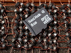
See also

[edit]

Notes

[edit]

References

[edit]
[edit]
Revisions and contributorsEdit on WikipediaRead on Wikipedia
from Grokipedia
Magnetic-core memory is a form of (RAM) that uses arrays of small, doughnut-shaped ferrite cores, each capable of storing a single bit of data through magnetic orientation—clockwise or counterclockwise—to represent binary 0 or 1. These cores are threaded with wires in a grid structure, enabling electrical currents to magnetize them for writing data and detect their state for reading, with access times as fast as 5 microseconds in early implementations. Non-volatile and reliable even without power, it dominated computer main memory from the mid-1950s to the mid-1970s, offering higher density, speed, and cost-effectiveness than prior technologies like vacuum-tube or mercury-delay-line storage. The invention of magnetic-core memory is primarily credited to Jay W. Forrester, an MIT engineer, who developed the practical coincident-current addressing scheme to efficiently select individual cores in a large array, filing a application on May 11, 1951, and receiving U.S. Patent 2,736,880 in 1956. This system was first operational in MIT's computer on August 8, 1953, where it provided 1024 words of storage at speeds capable of approximately 20,000 operations per second, marking the birth of reliable RAM for . Earlier ideas for core-based storage emerged in the late 1940s, including a 1949 by and Way-Dong Woo for a pulse-transfer device using ferrite cores, which Wang sold to for $500,000 in 1955 after legal settlements. Forrester's refinement, however, addressed scalability issues, reducing wire count and enabling dense planes of up to thousands of bits, with later paying MIT $13 million for rights in 1964. In function, writing data involves sending half-select currents through X and Y drive wires to fully magnetize a target core at their intersection, while reading uses a wire to detect induced voltage from the core's state change, followed by immediate rewriting to preserve data—a destructive readout process that ensured reliability. Its historical impact was profound, powering critical systems like the U.S. SAGE air defense network until 1983 and NASA's early space missions, including the , where core memory modules endured the 1986 Challenger explosion intact due to their ruggedness. By the 1970s, advancements in gradually replaced it, though core memory's legacy endures in the evolution of high-speed, random-access storage essential to modern .

Fundamentals

Core structure and magnetic principles

Magnetic-core memory employs small toroidal structures known as cores, fabricated from ferromagnetic materials, as the fundamental units for data storage. Each core functions as a single bit of memory, retaining information through the orientation of its internal magnetic domains—either clockwise or counterclockwise, corresponding to binary states 0 or 1. These toroids are arranged in a grid-like array, with wires passing through their centers to manipulate and detect the magnetic state. The design leverages the material's ability to maintain two stable remanent magnetization directions without external influence, ensuring non-volatile storage. The cores are primarily composed of ferrite, a semi-hard magnetic ceramic material with the general formula MFe₂O₄ (where M is a divalent metal such as or magnesium), particularly manganese-magnesium variants such as Ferroxcube 6D3, which exhibits low electrical conductivity to suppress losses during rapid switching. Typical dimensions in mid-20th-century designs measured approximately 1.3 inner diameter, 1.95 outer diameter, and 0.58 height, enabling dense packing in planes. The electromagnetic behavior of these cores is governed by the hysteresis loop of the ferromagnetic material, which is engineered to be nearly rectangular for reliable bistable operation. In this B-H curve, saturation magnetization BsB_s represents the maximum flux density achieved when an applied field fully aligns the magnetic domains through irreversible wall motion and rotation. Upon field removal, the core retains a high BrB_r (close to BsB_s), preserving the bit state at stable points on the loop. HcH_c denotes the reverse field intensity required to drive the to zero, typically low in these materials to facilitate switching with modest currents. This square-loop characteristic allows selective disturbance of cores via half-amplitude fields, forming the basis for coincident selection. To interact with the cores, fine wires—typically X and Y lines for addressing rows and columns, a wire for detecting induced voltage from reversal, and an inhibit wire for write precision—are threaded through the toroids in a woven matrix. Currents in these wires produce localized magnetic fields that traverse the loop, aligning domains to set or the state. The ferrite's , including high squareness (Br/Bs>0.9B_r / B_s > 0.9), ensure minimal disturbance to adjacent cores during operation.

Addressing and selection mechanisms

Magnetic-core memory primarily employed the coincident-current addressing scheme, invented by Jay Forrester in 1951, which utilized a rectangular array of ferrite cores threaded by X and Y drive lines to select individual cores efficiently. In this method, each X line ran horizontally through one row of cores, while each Y line ran vertically through one column, forming a grid where the intersection of a selected X and Y line targeted a specific core. To access a core, half-select currents—typically around 200 mA each—were applied simultaneously to one X line and one Y line, summing to a full-select current (approximately 400 mA) sufficient to switch the core's magnetic state, while half-select currents alone produced only minor loop excursions without full switching. This approach minimized wiring complexity, requiring only 2√N lines for an N-core plane, compared to N² lines in direct selection methods. Memory planes were organized either bit-wise or word-wise to accommodate data width. In bit-organized planes, each plane stored a single bit position across all addresses, with separate sense lines per plane to detect the output from the selected core. For multi-bit words, multiple such planes were stacked, sharing the X and Y drive lines but using individual sense and inhibit wires per plane; for example, the Whirlwind computer at MIT initially used stacks of 16 planes to form 16-bit words. In word-organized configurations, all bits of a word resided in a single plane, with inhibit lines threaded through cores to selectively prevent writing in non-target bits during word operations, enabling denser packing for wider words like the 36-bit formats in later systems such as the 704. Drive circuitry for X and Y lines typically incorporated matrices or transformers to steer currents and ensure precise timing, with positive currents (e.g., +200 mA half-select) for setting cores to one state and negative currents (e.g., -200 mA) for resetting to the other. Transformers allowed efficient current multiplication from fewer stages, reducing the number of active components from 2N to approximately 4√N for an N x N . Inhibit , often using similar or transistor-based circuits, applied opposing currents to unselected bits in a word to avoid disturbance during writes. To mitigate crosstalk and errors from partial selections, techniques such as three-dimensional (3D) selection extended the coincident-current method into stacked planes with Z-lines for additional discrimination, allowing larger arrays like 32x32x32 without increased per-core wiring. Linear selection addressed noise by weaving sense lines at 45-degree angles through the core array, canceling induced voltages from half-selected cores via geometric symmetry. These methods, combined with bias windings to stabilize minor loops, ensured reliable selection thresholds leveraging the cores' square hysteresis characteristics.

Operation

Reading process

The reading process in magnetic-core memory involves a destructive readout mechanism, where the application of a full magnetizing current to the selected core drives it toward the 0 state, flipping it if it stored a 1 (thereby destroying the original data) but causing minimal flux change if it already stored a 0. This occurs because the coincident currents along the X and Y wires produce a total sufficient to reverse the 's toward the 0 state only at their intersection. The changing during this reversal induces a voltage in the sense winding threaded through the core; a storing a 1 generates a larger positive (typically 10-50 mV) due to the full transition from saturation, while a core storing a 0 produces a much smaller or negligible signal as minimal flux change occurs. This induced sense voltage, being a differential analog signal on the order of millivolts, is detected by a dedicated that amplifies it to standard logic levels (e.g., from ~40 mV to several volts) for digital . The amplifier incorporates timing circuitry, such as strobing at the peak of the flux reversal (around 0.1-1.5 µs after current application), to sample the signal and distinguish it from noise. The output of the indicates the original bit value: a threshold-exceeding signifies a 1, while sub-threshold levels indicate a 0. The complete reading sequence begins with address selection, which activates the appropriate X and Y drive lines to half-select rows and columns, culminating in full selection of the target core. A read current pulse is then applied to drive the core toward 0, the sense signal is captured and amplified, and—since the readout is destructive—the original data bit is immediately rewritten to the core in a subsequent step to preserve the information. To ensure reliable detection, noise from partial flux changes in half-selected cores (which receive only half the magnetizing current and produce ~2 mV signals) must be minimized; this is achieved through the core material's nonlinear hysteresis characteristics, which prevent full switching under half-current, and by amplifier design that filters low-amplitude, mistimed disturbances.

Writing process

In magnetic-core memory, the writing process involves altering the magnetic state of a selected core to store a binary value, typically following a destructive read operation that resets the core to a known state. To write a "1," half-select currents are applied simultaneously to the intersecting X and Y drive lines of the target core, producing a full drive current in the positive direction to saturate the core's . For a "0," the same X and Y currents are applied, but an inhibit current is simultaneously driven through the inhibit wire threaded through the same cores on the sense line, opposing the X current and reducing the net below the threshold needed for saturation, thereby leaving the core in its reset state. The current levels are calibrated to ensure reliable switching without disturbing non-selected cores; each half-select current on the X or Y lines is approximately half the full required for the core material, typically on the order of hundreds of milliamperes at the intersection in ferrite cores. The write pulse is timed precisely, with a duration of about 1 µs to allow complete magnetic reversal while minimizing power dissipation and heat buildup in the array. Due to the destructive nature of reading, which resets the selected cores to "0" regardless of their prior state, every write operation must include a post-read rewrite phase to restore or set the intended data using the originally sensed value. The system's control logic latches the sensed output from the read and drives the inhibit lines accordingly during the subsequent write pulse, ensuring across the full read-modify-write cycle. To prevent errors such as accidental state flips in adjacent or half-selected cores, the inhibit mechanism precisely counters the drive currents only for the targeted bits, while the overall array design uses twisted or woven wire paths to minimize and inductive noise that could induce unintended magnetic fields. Sense amplifiers further aid in error-free operation by reliably detecting the small voltage pulses from core switching, allowing accurate determination of the pre-write state for rewriting.

Advanced operational cycles

In magnetic-core memory systems, the combined sense and inhibit operation optimizes wiring by integrating the and inhibit functions into a single wire, reducing the total from four to three wires per core while maintaining functionality during read and write cycles. This approach, patented in designs such as U.S. Patent 3,329,940, employs a center-tapped configuration where the wire serves as the line for detecting changes during reads and as the inhibit line by applying an opposing current from the center tap to prevent unwanted core flips during writes. For instance, in systems like the Burroughs 3-wire module, the sense/inhibit wire threads through blocks of 64 cores in a manner that parallels address wires in opposite directions, allowing induced currents to be canceled selectively without interfering with sensing. The combined read and write with modify cycle further enhances efficiency by performing a destructive read, immediate data modification in the processor, and restorative write within a single operational sequence, avoiding the need for separate full cycles. During this process, the read pulse—typically a negative half-amplitude current on the selected X and Y lines—drives the target core at their intersection toward the zero state, flipping it if it stored a 1, while half-selected cores experience minimal change, inducing a sense signal proportional to the original data bits; the processor then uses this sensed data to determine the write currents, applying full positive amplitude to restore ones and inhibit pulses (opposite current on the inhibit wire) to maintain zeros. In implementations like the , this integration ensures that the write phase follows the read without pausing for data latching, using opposite-polarity pulses on the selection lines to set the desired state. Timing in these advanced cycles relies on precisely overlapping pulses to minimize latency, with the read initiating flux reversal followed immediately by the write without intermediate delays, enabling the entire read-modify-write operation in as little as 1.2 microseconds in optimized systems. For example, the X-line precedes the Y-line by a short interval during sensing to separate induced currents, while the inhibit overlaps the write phase to block flips in non-target cores, as illustrated in drive circuit diagrams where durations of about 2 microseconds include rapid rise and fall times of 0.8 microseconds each. This overlap is critical in coincident-current arrays, where half-select currents sum vectorially at the target core, and any misalignment could cause disturb effects in adjacent cores. These optimized cycles provide significant advantages, particularly in halving effective access times for word-organized systems by merging the inherently destructive read with the required write restoration, compared to separate operations that would double the cycle duration. In two-dimensional (2D) linear-select arrays, where full currents are applied to word lines, the combined approach yields even greater efficiency than in three-dimensional (3D) coincident-current stacks, as it reduces complexity in larger matrices without increasing power dissipation or core disturb risks. Overall, such integrations were essential for real-time computing applications, enabling cycle times under 2 microseconds in megabit-scale memories while preserving non-volatility and reliability.

Variants

Standard coincident-current memory

The standard coincident-current magnetic-core memory organizes small ferrite cores into a two-dimensional matrix within each bit plane, where each core represents one bit of storage at the intersection of an X (row) and Y (column) selection wire. To select a specific core for reading or writing, half the required switching current is applied simultaneously to its corresponding X and Y wires, producing the full switching current only at that intersection while half-currents disturb but do not flip adjacent cores. Typical plane sizes ranged from 32×32 to 64×64 cores, storing 1,024 to 4,096 bits per plane, as seen in configurations like a 64×64 array using 128 select lines for efficient addressing. To achieve word lengths greater than one bit, multiple bit planes are stacked into a three-dimensional , with shared X and Y wires threading through all planes at the same coordinates, while separate and inhibit wires handle bit-specific operations across the stack. For instance, a 16-bit word would consist of 16 stacked planes, each contributing one bit position to every word in the , allowing simultaneous access to all bits of a selected word via coincident currents on the common drive lines. This architecture found widespread use in mainframe computers, such as the 7090, which employed up to 32,768 words of 36-bit core memory organized in stacked planes for high-speed scientific and applications. Power consumption was relatively low for the era, typically around 1 W per 1,024 bits, due to the pulsed nature of drive currents (e.g., 150–500 mA half-select pulses) and efficient hysteresis properties that minimized steady-state dissipation. However, scalability was constrained beyond approximately 64K words, as larger matrices demanded higher drive currents to overcome noise and disturbance effects from half-selected cores, increasing power requirements and complicating sense amplification without introducing errors.

Core rope memory

Core rope memory is a read-only variant of magnetic-core memory designed for permanent storage of fixed data, such as programs or constants, where information is encoded by the physical threading of wires through ferrite cores. In its construction, each core is surrounded by multiple address and inhibit wires for selection, along with numerous sense wires—one for each bit position in the stored words. A bit value of 1 is represented by threading a sense wire through the core, while a 0 is indicated by bypassing the core with the wire; this allows a single core to store multiple bits simultaneously, typically up to 192 bits in advanced implementations, enabling high-density storage. The assembly forms a "rope" of bundled wires and cores, often hand-woven and epoxy-potted for durability, with no provision for altering the wiring pattern post-construction. Operationally, core rope memory functions similarly to the reading process in rewritable core memory but lacks any writing capability, making it ideal for non-volatile, fixed-content applications in space-constrained or high-reliability systems. To read a word, address lines activate inhibit wires to select a specific core via coincident-current selection, applying set and reset pulses to induce changes; the resulting voltage pulses on the threaded sense wires are detected in parallel to output the encoded bits. This process yields outputs around 200 mV with a high , completing in cycles of approximately 11.7 µsec, though the fixed wiring ensures without risk of overwrite. A prominent example is the (AGC), where served as the fixed read-only storage for the spacecraft's navigation and guidance software. The AGC employed six rope modules, each with 512 cores storing 12 words of 16 bits (including parity), totaling 36,864 words or approximately 72 kilobytes of ROM, complementing 2,048 words of erasable memory. Programs were translated from to wire patterns via perforated tapes guiding the weaving process, often performed by skilled women assemblers. The design offered key advantages, including exceptional density—up to 1,500 bits per , five times that of contemporary erasable core memory—making it suitable for embedding constants and immutable in compact systems. Additionally, the ferrite cores and encapsulation provided strong resistance to and environmental hazards, ensuring reliability in extraterrestrial conditions without power dependency for .

Other specialized forms

Word-line memory, also known as linear select or word-organized core memory, employs a dedicated selection wire for each word rather than the half-current coincident selection of standard designs. This approach delivers full selection current to the target word line, minimizing and half-select disturbances that can degrade in dense arrays. By integrating steering for line selection, it enables faster access times suitable for high-speed registers and cache-like structures, as demonstrated in a 8192-word, 54-bit system achieving cycle times under 2 microseconds. Three-dimensional core stacks extend the planar coincident-current architecture by layering multiple planes of cores vertically, with a common inhibit or Z-wire threading through all planes to select individual layers. This configuration, pioneered by Jay Forrester, allows one core per bit in a cubic array, dramatically increasing density while sharing X and Y drive lines across planes to reduce wiring complexity. Early implementations supported military applications, such as air defense systems requiring compact, reliable storage for several million bits. Twistor memory represents an evolutionary departure from discrete toroidal cores, utilizing a continuous fine wire (typically 0.005 inches in ) coated with a thin magnetic , around which helical windings are applied. Writing orients the film's magnetization via toroidal fields from current in the wire, while reading induces signals nondestructively through flux changes detected by lines. Compared to traditional core , twistor achieves higher packing density with simpler automated fabrication, lower power requirements, and equivalent access speeds around 1 , making it viable for large-scale switching systems.

Performance and Physical Properties

Speed and capacity characteristics

Magnetic-core memory systems in the early typically operated with cycle times of 6 to 12 microseconds, enabling that was significantly faster than preceding technologies like electrostatic storage tubes, which required around 10 microseconds. By the late , access times had improved to under 10 microseconds, supporting applications such as those in the computer. These early performance levels were achieved with ferrite cores approximately 2 millimeters in diameter, driven by currents of 400 to 800 milliamperes. Advancements through the 1960s and into the 1970s reduced cycle times dramatically, reaching 1.2 microseconds by the early 1970s and 600 nanoseconds by the mid-1970s, primarily due to smaller core sizes—shrinking to about 0.4 millimeters in diameter—and improved circuits that provided sharper current pulses. For instance, the Model 40 utilized read/write pulses lasting 400 to 700 nanoseconds, contributing to its effective access speeds. The core switching process, which involves reversing the , typically took 1 to 5 microseconds depending on ferrite quality, while wire in the plane introduced delays in current rise times, limiting overall speed. Switching time was proportional to core size, as larger cores required more time for flux reversal due to higher magnetic . The cycle time in these systems can be approximated as tcycle2×(trise+tflip)t_{\text{cycle}} \approx 2 \times (t_{\text{rise}} + t_{\text{flip}}), where triset_{\text{rise}} is the of the drive current influenced by wire and tflipt_{\text{flip}} is the core flip time determined by the loop characteristics of the ferrite material. In terms of capacity, early implementations like the computer featured around 8,192 words of core memory, equivalent to roughly 128 kilobits assuming 16-bit words, marking a substantial increase from initial prototype planes of 1,024 bits. Large-scale systems by the 1960s, such as the , supported up to 256 kilobytes in typical configurations, with high-end models reaching 2 megabytes or more through stacked planes. Bit density hovered around 1 bit per square millimeter in mid-1960s designs, limited by the grid spacing needed for wiring and core placement, though this scaled to higher densities in later miniaturized arrays before the technology's obsolescence in the late 1970s. Over its lifespan, capacities evolved from kilobit scales in the to megabit levels in production systems, balancing speed improvements with practical manufacturing constraints.

Reliability and environmental factors

Magnetic-core memory exhibits non-volatility, retaining stored data indefinitely without , a property that made it suitable for applications requiring persistent storage. This characteristic stems from the in ferrite cores, where states remain stable post-write operation. Furthermore, its robustness to positioned it as a preferred choice for and systems; core memory was deployed in over 2,000 and units due to its resistance to radiation-induced errors, unlike alternatives vulnerable to single-event upsets. Failure rates for magnetic-core memory systems were notably low, with (MTBF) exceeding hundreds of thousands of hours in operational environments. For instance, all-magnetic systems incorporating core memory achieved an MTBF of approximately 369,000 hours, where the cores themselves contributed minimally to overall compared to supporting like transistors and diodes. The inherent reliability of the cores—far surpassing associated components—enabled redundant designs that boosted system reliability by over 300 times for one-year operations, as typically defaulted to a safe "zero" state without cascading effects. Common failure modes included mechanical issues such as core cracking from or mechanical stress and wire from repeated current pulses, though these were rare and often mitigated through quality manufacturing. Temperature sensitivity posed a challenge, as the of ferrite cores decreases with rising temperature, altering the loop and reducing the current required for flux switching—potentially leading to errors if unaddressed. Compensation circuits addressed this by incorporating temperature-sensitive resistors in driver current sources and power supplies for X-Y and Z lines, ensuring consistent inhibit and select currents; core-derived strobing further stabilized timing against variations. Environmental resilience was a key strength, with potting compounds encapsulating core stacks to enhance tolerance to shock and , allowing reliable performance in rugged applications like . Compared to semiconductors, core memory offered resistance in (EMP) scenarios, as its mechanism was less affected by transient fields that disrupt electronic circuits.

Diagnostics and maintenance

Diagnostics of magnetic-core memory systems typically began with built-in tests to verify core functionality and detect faults such as stuck bits. These tests employed patterns like all-zeros and all-ones writes followed by reads to confirm proper switching, with sense line outputs monitored for expected voltage pulses around 35-40 mV lasting approximately 600 ns. Marching patterns, where a single bit is stepped through the array while writing and reading 0s and 1s, helped identify addressing errors or weak signals from marginal cores. Checksums or parity checks were integrated in systems with parity bits to detect multi-bit errors during operation. Visual inspection was essential for assessing physical integrity, involving checks for core alignment in the weave pattern, wire tension and integrity, and joint quality. Misaligned cores or loose wires could cause incomplete , leading to unreliable switching. Tools such as oscilloscopes were used to verify drive pulse waveforms and responses, ensuring half-select currents (typically 150-500 mA) produced clean signals without excessive noise from or half-selected cores. Repair techniques focused on targeted fixes to minimize . For defective individual cores, identified during testing as non-switching or producing weak sense signals, the faulty core was crushed with a , the threading wires retracted, a replacement core inserted from a spare supply, and wires rethreaded before retesting the plane. Wire faults required affected sections, rethreading through the core array, and resoldering, often using automated winding machines for precision in larger arrays. In cases of widespread issues, such as faulty decoding logic or corroded connectors, entire memory planes or control cards were replaced after cleaning for dirt and corrosion. Common faults included shorted or frayed sense lines, which induced noise spikes mimicking false reads, and demagnetized or fatigued cores resulting from overdriving currents or prolonged exposure to high temperatures that distorted the hysteresis loop. Preventive emphasized environmental controls, such as cooling to maintain core temperatures below levels that shifted B-H curve characteristics, and periodic current adjustments to avoid buildup during high-repetition testing rates around 1 kHz.

History and Development

Early development and key contributors

The development of magnetic-core memory emerged as a response to the shortcomings of prior technologies, including mercury delay lines, which offered serial access but suffered from temperature sensitivity and limited capacity, and Williams-Kilburn tubes, which provided via cathode-ray tube storage but were volatile and prone to signal decay. In October 1949, , a physicist at Harvard University's Computation Laboratory, filed U.S. Patent No. 2,708,722 for a "pulse transfer controlling device" that utilized small ferrite cores in a serial configuration to store and transfer binary pulses through , enabling non-destructive readout. This invention addressed the need for a reliable, compact alternative to electrostatic storage by exploiting the square hysteresis loop of ferrite materials to represent 0s and 1s as opposing magnetic orientations. Independently, between 1951 and 1953, Jay Forrester and his team at MIT's Project Whirlwind implemented the first operational magnetic-core memory system for real-time computing applications, such as flight simulation for the U.S. Navy. Forrester filed U.S. Patent No. 2,736,880 in May 1951 for a multicoordinate digital information storage device using three-dimensional arrays of ferrite cores, which allowed efficient selection of individual bits via half-currents along X, Y, and Z axes to minimize wiring complexity. The Whirlwind I became the first computer to run with core memory in August 1953, initially equipped with 1,024 16-bit words and expandable to 4,096 words, demonstrating reliable operation at speeds up to 17 microseconds per access cycle. Concurrently in 1952, Jan A. Rajchman at RCA Laboratories advanced core memory design through experiments with static magnetic matrix arrays, as detailed in his publication "Static Magnetic Matrix Memory and Switching Circuits" that optimized core selection for high-density storage. Rajchman's work, building on his 1950 patent application for magnetic storage devices, emphasized toroidal cores and inhibit windings to reduce crosstalk in larger matrices, achieving early prototypes with up to 10,000 bits. These efforts paralleled ongoing research at Harvard under Wang and at the University of Manchester, where engineers like Tom Kilburn explored core adaptations following their success with Williams tubes, leading to integrated systems by 1953.

Patent disputes and commercialization

The development of magnetic-core memory faced significant patent interferences in the early , primarily involving key inventors such as , Jay Forrester, and Jan Rajchman from RCA. Wang filed a for a pulse transfer controlling device using magnetic cores in 1949, which was granted in 1955 (US 2,708,722), addressing efficient reading of magnetically stored data without destructive readout in serial configurations. Forrester applied for his on the coincident-current random-access core memory system in 1951, granted in 1956 (US 2,736,880), enabling scalable 3D arrays for high-speed access. Rajchman, working at RCA, pursued similar claims for core-based storage, leading to an interference proceeding with Forrester's application; the U.S. Patent Office declared interference, but Rajchman conceded Forrester's priority of invention, resulting in RCA withdrawing its claims around 1956. To facilitate commercialization amid these disputes, licensing agreements were established. In 1955, Wang sold his core memory patent rights to IBM for $500,000, providing IBM with foundational technology for non-destructive readout integration. MIT, holding Forrester's patent, granted RCA access through a hybrid royalty-free and royalty-bearing license following the interference resolution, allowing RCA to produce core memory without further litigation. These arrangements, including cross-licensing elements among MIT, RCA, and emerging users, cleared paths for industry-wide adoption by 1956, though broader disputes persisted. IBM led early commercialization, integrating core into its systems as a superior alternative to unreliable electrostatic storage tubes. The , announced in 1954 and delivered starting in 1955, was the first commercial computer to use magnetic-core main , offering 4,096 to 32,768 words at 12-microsecond cycle times, marking a shift from vacuum-tube-based electrostatic prone to failure. This adoption accelerated with the 1956 , the first commercial system combining core for primary storage with random-access disk drives, enabling efficient for business applications. Widespread industry adoption followed, supplanting electrostatic and delay-line storage due to core memory's reliability and speed. Sperry Rand's , delivered in 1958, employed core memory for its scientific computing lineup, replacing earlier drum and tube systems in military and research uses. Ferranti's Mercury computer, introduced in 1957, incorporated core memory for high-performance tasks, contributing to the technology's dominance in European systems. By the late 1950s, these implementations drove a rapid transition, as core memory's non-volatility and resistance to radiation made it ideal for defense projects like SAGE. Ongoing patent conflicts culminated in 1964, when settled with MIT for $13 million in rights to Forrester's patent—the largest such agreement at the time—solidifying core memory's commercial foundation.

Production economics and decline

The production of magnetic-core memory was initially highly labor-intensive, requiring manual of fine wires through arrays of tiny ferrite cores, a process that significantly contributed to high costs. In the , each core, representing one bit of storage, cost approximately $1 due to the handmade assembly and limited-scale ferrite production. By the early , advancements in , including mechanized winding machines such as needle feeders and semi-automatic X-Z feeders developed by , began to automate the threading and testing processes, reducing assembly time from 120 hours per megabit to as little as 1 hour. Bulk production of ferrite cores also drove ; for instance, General Ceramics increased output to 250,000 cores per day by 1959, lowering individual core costs from 50 cents to 3 cents through improved yields (from 30% to 98%) and optimized pressing and firing techniques. These efficiencies, combined with smaller core sizes, further reduced the overall cost per bit to about $0.01 by 1970. The decline of magnetic-core memory accelerated with the introduction of (DRAM) technology, particularly Intel's 1103 chip in 1970, which offered 1,024 bits at a launch price of $60—or roughly 5.9 cents per bit—while being significantly smaller, lighter, and less power-hungry than core memory equivalents. Although initial DRAM access times were comparable or slightly slower than core's 1-microsecond cycles, the semiconductor approach enabled rapid scaling and cost reductions that core production could not match, leading to core memory being phased out in most minicomputers by 1975, as seen in systems like the series transitioning to in 1974. Despite this, core memory persisted in legacy applications into the 1980s and beyond, notably in systems such as the IBM 9020 used by the FAA until the late 1990s for its proven reliability in critical environments.

Legacy and Impact

Applications in historical computing

Magnetic-core memory played a crucial role in enabling and reliable in several landmark systems during the mid-20th century. Its non-volatility, resistance to , and robustness in harsh environments made it ideal for applications where was paramount, from defense to scientific simulations and . The computer, which became operational in 1951 at MIT using initial electrostatic memory, was one of the first to implement magnetic-core memory in 1953, developed by Jay Forrester, which allowed for real-time control capabilities essential to the SAGE () air defense system. SAGE, deployed in the 1950s and 1960s, used Whirlwind-derived core memory in its AN/FSQ-7 processors to track and intercept potential aerial threats across , processing radar data in milliseconds for Cold War-era continental defense. This application demonstrated core memory's ability to handle high-speed, interrupt-driven operations in a networked environment, influencing subsequent military computing designs. In scientific computing, the 7090, introduced in 1959, utilized core memory with a 2.18-microsecond cycle time, supporting complex numerical simulations for research institutions and government projects. This system was instrumental in NASA's , where dual IBM 7090s at mission control processed telemetry data, trajectory calculations, and real-time monitoring for the first U.S. manned spaceflights from 1961 to 1963, ensuring precise orbital insertions and safe re-entries. The follow-on series, launched in 1964, also employed core memory across its models, facilitating large-scale scientific workloads in fields like physics and , with capacities up to 512 kilobytes that enabled multiprogramming and for the space program and beyond. In space exploration, core memory was used in the Space Shuttle's onboard computers for critical flight control systems, demonstrating its robustness as modules survived the 1986 Challenger disaster intact. Minicomputers like the PDP-8, released in 1965, incorporated core memory for its proven reliability in laboratory environments, where frequent power cycles and vibrations were common. With up to 32 kilobytes of core storage, the PDP-8 powered instrumentation control, , and process in research labs worldwide, becoming the best-selling computer of its era due to its compact design and fault-tolerant memory that retained data without backup power. Specialized applications leveraged core memory's non-volatility in extreme conditions, such as the AN/UYK-7 computer deployed in U.S. Navy submarines starting in the 1970s, which used 100 kilobytes of core storage to manage processing and without during power interruptions or underwater operations. Similarly, telephone switching systems like North Electric's Omni series in the 1960s and 1970s employed core memory for call routing and billing records, ensuring uninterrupted service in remote or power-unstable telecom installations. For the , core-based rope memory stored fixed guidance software in the onboard computer, complementing rewritable core variants in ground systems.

Comparisons to modern memory technologies

Magnetic-core memory, while revolutionary in its era, differs markedly from (DRAM) in key attributes such as volatility, speed, , and environmental resilience. Unlike DRAM, which stores data as electrical charges in capacitors and requires periodic refreshing to prevent loss, core memory is inherently non-volatile, retaining information without power due to the stable magnetic states in ferrite cores. However, core memory's access times typically ranged from 1 to 2 microseconds, far slower than modern DRAM's nanosecond-scale operations, limiting its scalability for . Additionally, core memory's wire-woven structure made it bulkier and less dense than DRAM, which achieves gigabit-scale capacities in compact chips through fabrication. In terms of reliability, core memory exhibited superior , making it suitable for harsh environments, whereas DRAM is more susceptible to single-event upsets from cosmic rays. Comparisons with static random-access memory (SRAM) and further highlight core memory's mechanical robustness against electronic degradation. SRAM, used for high-speed caches, offers sub-nanosecond access without refresh cycles but remains volatile and consumes more power per bit than core memory's low standby requirements; its transistor-based cells also generate more heat, contrasting core memory's passive . , a non-volatile alternative, provides higher density and lower cost for but suffers from write limitations—typically 10,000 to 100,000 cycles per cell—due to wear, while core memory demonstrated virtually unlimited read/write cycles without degradation, relying on durable ferrite materials rather than electrical stress. This mechanical reliability gave core memory an edge in long-term , though its larger physical footprint and higher fabrication complexity made it uneconomical compared to flash's solid-state efficiency. Contemporary memory technologies like magnetoresistive (MRAM) echo core memory's magnetic principles, aiming to combine non-volatility with speeds. MRAM stores data via magnetic tunnel junctions, similar to how core memory used toroidal for binary states, but replaces bulky wires with nanoscale spintronic elements for densities approaching DRAM. Early MRAM concepts in the directly sought to miniaturize core memory's toroids using magnetoresistive sensing, evolving into commercial products that offer endurance exceeding 10^15 cycles and radiation tolerance. Despite its obsolescence, core memory's advantages in radiation hardness and non-volatility have been retained in some legacy military and space systems, such as the (retired in 2011), where upgrades were deemed costly or risky. This retention underscores core memory's foundational role in designing resilient storage for extreme environments.

References

Add your contribution
Related Hubs
Contribute something
User Avatar
No comments yet.